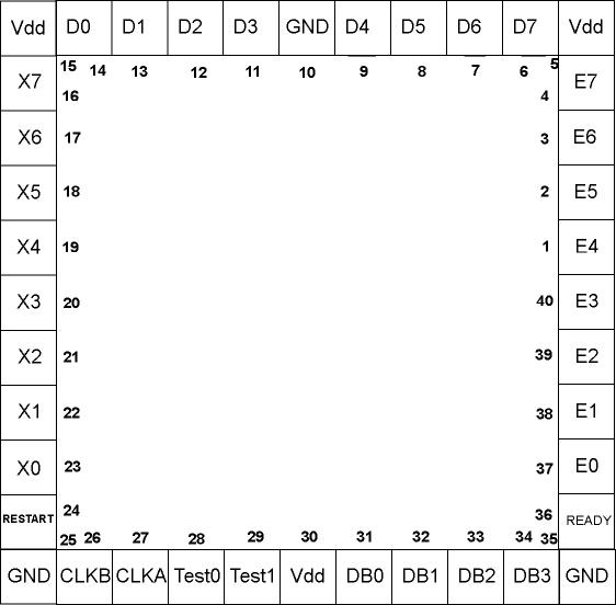
Overview
| Pin Name | Number of Pins Required | Physical Pin Number | Signal Type | Description |
| Vdd / GND |
6 |
5, 10, 15, 25, 30, 35 |
Power |
Supplies power and ground to the chip |
| CLKA | 1 | 27 | Input | 2 Phase Clock A |
| CLKB | 1 | 26 | Input | 2 Phase Clock B |
| RESTART | 1 | 24 | Input | Signal for resetting PLA and clearing all Latches |
| X[7:0] | 8 | 16-23 | Input | Noise reference input |
| D[7:0] | 8 | 6-14 | Input | Input signal containing noise |
| E[7:0] | 8 | 37-40, 1-4 | Output | Final filtered output signal |
| DB[3:0] | 4 | 31-34 | Output | Debugging Output Pins (multiplier output latch, adder output latch) |
| Test[0:1] | 2 | 28-29 | Input | Debug Control inputs to select which output to debug |
| READY | 1 | 36 | Output | A/D Converter Handshaking output |
Total Pin Count: 40
Pin Labelling in MOSIS Pad Frame
