
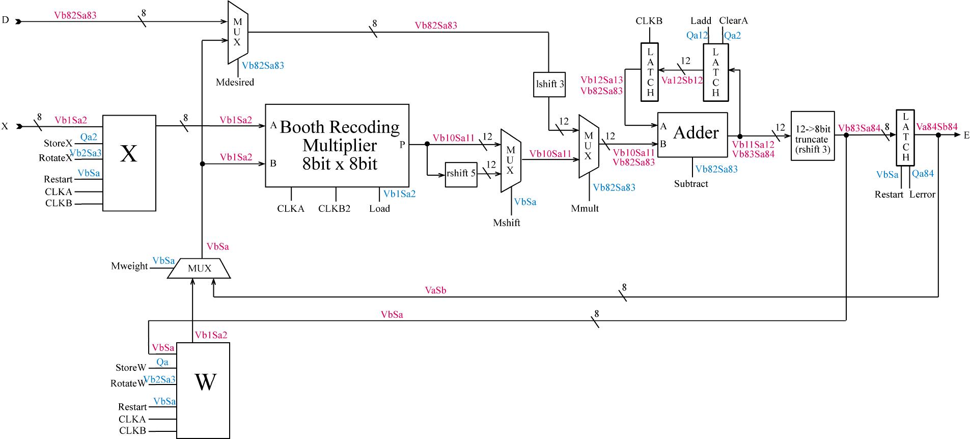
In this section we present the timing of our chip along with explanations of how the chip works according to the timing discipline. Our chip is being implemented with a two phase non-overlapping clocking scheme as described in papers by Karplus and Noice [1]. In this section we present the general timing of the entire system presenting only the required strengths of the signals. We present the exact timing with durations for each of the two separate, distinct phases of the computation in the system. Finally, we present the timing required inside the multiplier to produce one output from a set of inputs.
The diagram below presents the general system timing with only the minimum strengths required of the input and control signals in order to have valid operation.
The diagram below presents the timing for the system in the error calculation phase of the FIR filter process.
The diagram below presents the timing for the system in the weight update phase of the FIR filter process.
