
The arithmetic logic unit performs six functions - add, subtract,
logical AND, logical OR, shift left and shift right on 4-bit two's
complement binary numbers. The inputs to be calculated come from
the A Register (AREG) and the Accumulator (ACCUM) for add, sub,
AND and OR. The shift left and shift right functions operate
on the value in the ACCUM..
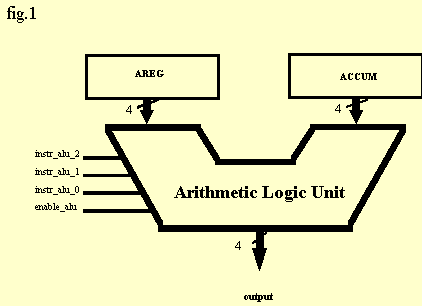
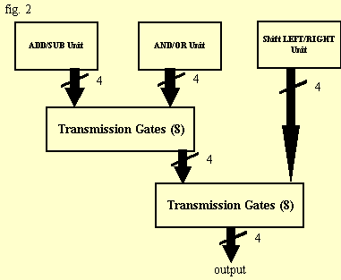
Figure 1 illustrates the functional level block diagram of the
ALU designed for the BOMB! The ALU is divided into three modules
(fig. 2) - the AND/OR unit, the ADD/SUB unit, and the shift left/right
unit.
REGISTER TRANSFER LEVEL DESCRIPTION
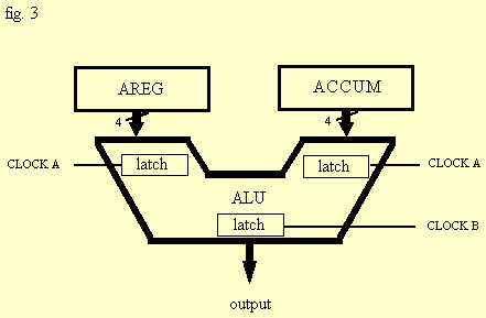
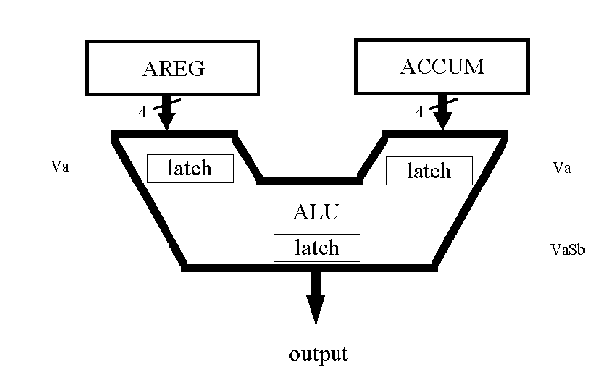
Data is always on the inputs and outputs of the ALU. Due to the
use of a two-phase non-overlapping clock we can insure valid outputs.
The inputs are latched on the rising edge of CLOCK A and the
outputs are latched on the rising edge of CLOCK B to allow the
signals time to propagate through the entire circuit. Figure
3 indicates how the registers are tied to the ALU and the clocking
required for calculations. The PLA sends a 3-bit instruction
indicating one of the six functions. The ALU decodes this instruction
and outputs on the rising edge of CLOCK B.
GATE LEVEL DESCRIPTION
AND/OR Unit
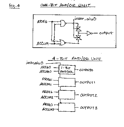
The AND/OR unit is composed of four one-bit AND/OR selection units
(fig. 4). The transmission gates select between AND and OR by
the instr_alu0 signal from the controller. When the instr_alu0
signal is high, the transmission gates allow the NANDed signal
through. When the instr_alu0 signal is low, the transmission
gates allow the NORed signal through. The output of the transmission
gate is then inverted to obtain the desired AND/OR output. The
AND/OR output will be selected by another set of similar transmission
gates between the AND/OR unit and the ADD/SUB unit.
ADD/SUB Unit
The one-bit carry-lookahead adder (fig. 5) is replicated and tied together to produce the four-bit adder for two's complement numbers. This allows addition of negative numbers which will serve to simplify the implementation of the subtraction function. The CARRY bit must propagate through each one of the one-bit adders in order to produce a valid output for alu_out_3. The ALU subtracts the AREG from the ACCUM.
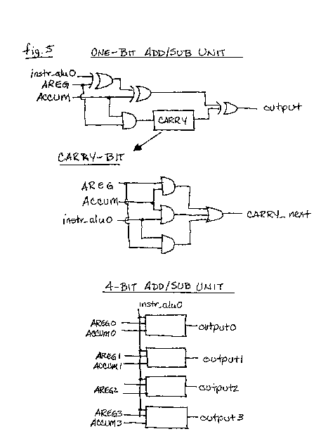
Subtraction with 2's complement numbers is simply two steps:
Negating the value in AREG makes it possible now to simply add
it to the value in ACCUM, in essence subtracting.
To invert each bit in AREG, they are XORed with a high input from
the PLA. In order to add a one to the answer, the CARRY bit must
also be high. Thus, the same instr_alu0 input can be used to
completely indicate the operation. When instr_alu0 is low, the
operation is a ADD with the value in AREG XORed with a 0 and the
CARRY bit being a 0 as well. When the instru_alu_0 is high, the
operation is SUB with the value in AREG XORed with a 1 changing
it to -AREG and the CARRY bit being a 1, adding one to the value.
The outputs are tied to the other side of a set transmission
gates which will select between the AND/OR output or the ADD/SUB
output. The instru_alu_1 selects which set of transmission gates
to send. This output will then be sent to another set of transmission
gates which will determine the final output of the ALU, selecting
between the three subunits.
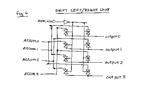
Shift Left/Right Unit
The barrel shifter (fig. 6) shifts the binary number from ACCUM
left or right by tying the inputs to two sets of transmission
gates. The instr_alu0 selects which set of transmission gates
which determines which direction to shift. The original inputs
are ABCD in that order. One set of transmission gates has them
in the order BCDA (shift left) and the other set is in the order
DABC (shift right). In building this subunit it is important
to keep track of the wires. The outputs of the transmission gates
are then tied to the last set of transmission gates in the ALU.
This set of transmission gates selects between the output of
the first subunit selector and the output of the barrel shifter.
The final output is then routed to a set of latches which will
be latched on the rising edge of CLOCK B. The ALU's output is
then routed to the bus where the controller will determine the
next destination.
ALU TIMING ANALYSIS
The ALU has two sets of latches for the inputs from the AREG and
the ACCUM. These inputs must be valid through the rising and
falling edge of CLOCK A, making it Va. All of the subunits within
the ALU are combinational logic which does not affect the timing.
The outputs of the ALU are latched on CLOCK B to ensure valid
signals. The outputs are VaSb coming out of the
fig. 8
ISSUES
ALU
Originally the ALU was to be separate from the barrel shifter.
Each unit would have had an extra control signal indicating a
pass through. If the instruction was shift left, the data from
the A register would have to pass through the ALU. Likewise,
if the instruction was an add, the data would have to pass through
the barrel shifter. Both the ALU and the barrel shifter would
require a bus controller. In order to be more space-efficient,
I incorporated the barrel shifter into the ALU which only required
adding another set of transmission gates to select between the
shifter's output and the original ALU's output.
After viewing other groups' layout, it seems that perhaps the
use of modular design is more space consuming. However, it made
testing and verifying the functionality of each subunit much simpler.
Debugging one module fixed all occurrences in the design.
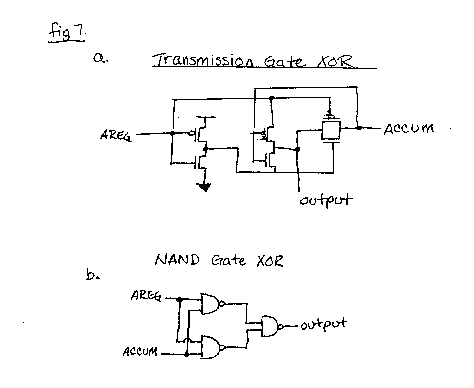
ADD/SUB Unit
The XOR gate (fig. C7a) is the most basic element of the Adder.
There are several different methods of building an XOR gate.
The first XOR gate was built with transmission gates. This proved
to be an unstable gate. Whenever transmission gates are used
to drive another input of another gate, buffers are needed to
stabilize the output. Transmission gates have no definite power
or ground, so the transistors can be unstable. The outputs on
the one-bit adder was correct. However, when four of them were
tied together, the CARRY-bit was unable to propagate through the
entire circuit in time for the output. Adds without CARRY's performed
fine. Once the CARRY bit had to propagate, the outputs which
required the CARRY bit of the four-bit adder were invalid.
The other form of the XOR gate (fig. C7b) turned out to be much
more stable. It is made up of three NAND gates and two INVERTERS.
Both of these gates have a distinct power and ground. The outputs
for the 4-bit adder were fine after switching out the XOR gate.
The new XOR gate was close to the same area as the original one,
so there was no loss of space.
Substrate Connections
Substrate connections are only necessary for the p-transistors
to prevent latch-up in our design. Adding substrate connections
to all of the transmission gates would have been a real challenge
, but fortunately, the design for the ALU was not extremely,.
The configuration selected for some of the transmission gates
was originally chosen to facilitate selection by the PLA's signal.
It turned out to make the substrate connections very erratic.
However, it did not take too much time to add them, and the final
design managed to have the same area.
| Back to the front page | On to next page... |