Indestructible This Time!

FUNCTIONAL DESCRIPTION
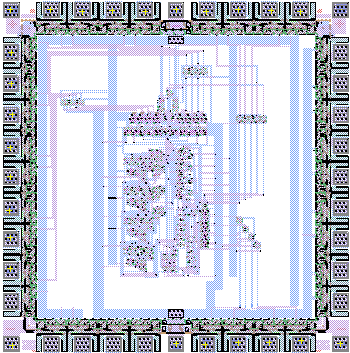
The BOMB! is a simplified ALU that has the basic functionality
of a simple calculator. The chip can add, subtract, and, or, shift
left, and shift right. It has two registers from which values
to be performed on are loaded into. The result of the operation
is not stored in a register, instead it is directly outputted
on the output lines.
The chip also takes two clock inputs in order to correctly latch
the inputs and outputs of the ALU.
ISSUES
The simplicity of the chip and the lack of more complex functions
is a result of the very limited amount of time we had. The goal
in creating this chip was to guarantee we had a working chip in
as little time as possible. The chip, while simple, is completely
functional.
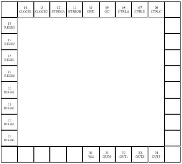
INSTRUCTION SET SPECIFICATION
The ALU can do 6 different operations. The arithmetic and logical
instructions all operate on the values in register A and register
B. The shift operations only operates on the value in register
B.
In order to load a value into the registers, the STREGA and STREGB
signals must be toggled high. The GO signal is used to correctly
latch both the inputs to the ALU as well as the outputs.
A sample sequence of operations is as follows:
| OPCODE | INSTRUCTION | DESCRIPTION | ||
| ARITHMETIC/LOGICAL | ||||
| 000 | ADDs the value in the register to the value on the accumulator and places the result in the accumulator | |||
| 001 | SUBTRACTs the value in the register to the value on the accumulator and places the result in the accumulator | |||
| 010 | Performs a logical AND on the value in the register to the value on the accumulator and places the result in the accumulator | |||
| 011 | Performs a logical OR on the value in the register to the value on the accumulator and places the result in the accumulator | |||
| 100 | SHIFTS the binary value in the register to the left by one and places a zero in the LSB | |||
| 101 | SHIFTS the binary value in the register to the right by one and places a zero in the MSB | |||
| Back to the front page | That's all! I hope you enjoyed the BOMB! Send comments to Christine Pan |