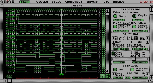
2nd Third of Results
Last Third of Results
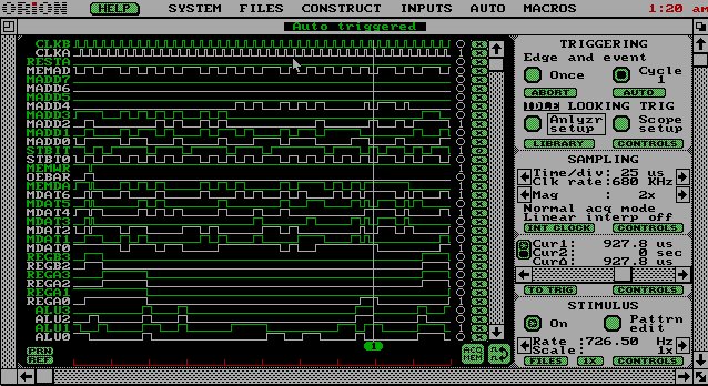
We verified the correctness of our chips by observing the store word values written back to memory which were supposed to be the negated values of the original array values that were loaded in. More importantly we observed the load word instruction which asks for the value at address x10. This load word instruction shows that the program correctly acknowledged that the memory register had to be incremented after x0F was loaded. We also verified instructions fetched, PC, and register outputs.
Chips 2, 4, and 5 all passed this test with complete functionality.
Program Code:

0  LDI   1110
1  OR    0111  // reg1 will be holding the address offset

loop:

2  LDI   0001
3  SETM  1011  // set MemReg for the data memory access
4  LW    0001  // reg0 <= next element of array
5  SETMI 0000  // set MemReg for the coming instruction memory access
6  NOT   0000  // reg0 <= !$reg0
7  ADD   0011  // $reg0++
8  SW    0001  // store the negate value back to the array
9  ADD   0111  // increment the address offset

10 LDI   0010
11 BGZ   0111  // branch if the offset is greater than zero
12 ZERO  0000
13 SUB   0001  // reg3 <= -offset
14 LDI   0010
15 BGZ   0111  // branch if offset is less than zero

16 LDI   0001
17 ADD   1011  // increment reg2 which holds the upper nibble for MemReg
18 ZERO  0000
19 LDI   0010
20 BEZ   0011  // goto loop
2nd Third of Results
Last Third of Results
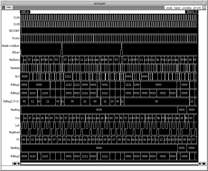
The relevant data is tough to pick out, and it would probably not help to have more plots. The key result is the setting of the MemReg to 01. This indicates that software has correctly traversed the 4-bit data memory segments.
clock Vdd      1 1 1 1
clock CLKA     0 1 0 0
clock CLKB     0 0 0 1

| pin vectors
vector MemData MemData7 MemData6 MemData5 MemData4 MemData3 MemData2 MemData1 MemData0
vector iMemData iMemData7 iMemData6 iMemData5 iMemData4 iMemData3 iMemData2 iMemData1 iMemData0
vector MemAdd  MemAdd8 MemAdd7 MemAdd6 MemAdd5 MemAdd4 MemAdd3 MemAdd2 MemAdd1 MemAdd0
vector iMemAdd  iMemAdd8 iMemAdd7 iMemAdd6 iMemAdd5 iMemAdd4 iMemAdd3 iMemAdd2 iMemAdd1 iMemAdd0
vector State   StBit0 StBit1
vector RdReg1 RegA3 RegA2 RegA1 RegA0
vector RdReg232 RegB3 RegB2
vector ALU ALU3 ALU2 ALU1 ALU0

| pin ana's

ana CLKA CLKB Restart MemAdd  State MemWriteQbar OEbar MemData RdReg232
ana RdReg1 ALU Vdd
ana Trigger

ana ILOAD WE_L iMemData


V RESTART   0
V iMemAdd  000000000 000000000  000000000 000000001 000000001 000000001 000000010 000000010 000000010 000000011 000000011 000000011
V ILOAD     0
V ILOAD_bar 1
V WE_L      1 0 1  1 0 1  1 0 1  1 0 1
V iMemData 11001110 11001110 11001110 00110111 00110111 00110111 11000001 11000001 11000001 11101011 11101011 11101011
R
V iMemAdd  000000100 000000100  000000100 000000101 000000101 000000101 000000110 000000110 000000110 000000111 000000111 000000111
V iMemData 11010001 11010001 11010001 10000000 10000000 10000000 01100000 01100000 01100000 01010011 01010011 01010011
R
V iMemAdd  000001000 000001000  000001000 000001001 000001001 000001001 000001010 000001010 000001010 000001011 000001011 000001011
V iMemData 10010001 10010001 10010001 01010111 01010111 01010111 11000010 11000010 11000010 10110111 10110111 10110111
R
V iMemAdd  000001100 000001100  000001100 000001101 000001101 000001101 000001110 000001110 000001110 000001111 000001111 000001111
V iMemData 11110000 11110000 11110000 00010001 00010001 00010001 11000010 11000010 11000010 10110011 10110011 10110011
R
V iMemAdd  000010000 000010000  000010000 000010001 000010001 000010001 000010010 000010010 000010010 000010011 000010011 000010011
V iMemData 11000001 11000001 11000001 01011011 01011011 01011011 11110000 11110000 11110000 11000010 11000010 11000010
R
V iMemAdd  000010100 000010100 000010100 100001110 100001110 100001110 100001111 100001111 100001111 100010000 100010000 100010000
V iMemData 10100011 10100011 10100011 11111110 11111110 11111110 11111101 11111101 11111101 11111100 11111100 11111100
R

V RESTART   0 0 0 0 0 0 0 0 0 1 0 0
V ILOAD     0 0 0 0 0 0 0 1 1 1 1 1
V ILOAD_bar 1 1 1 1 1 1 1 0 0 0 0 0
V WE_L      1 0 1 1 1 1 1 1 1 1 1 1
V iMemAdd  100010001 100010001 100010001 111111111 111111111 111111111 111111111 111111111 111111111 111111111 111111111 111111111
V iMemData 11111011 11111011 11111011 11111111 11111111 11111111 11111111 11111111 11111111 11111111 11111111 11111111
R

V ILOAD     1 1 1 1 1 1 1 1 1 1 1 1 1 1 1 1 1 1 1 1 1 1 1 1 1 1 1 1 1 1 1 1 1 1 1 1 1 1 1 1 1 1 1 1 1 1 1 1 1 1 1 1 1 1 1 1 1 1 1 1 1 1 1 1 1 1 1 1 1 1 1 1 1 1 1
V ILOAD_bar 0
V WE_L    1
V iMemAdd  111111111
V iMemData 00000000
V RESTART 0
R