Elec
422: VLSI Design I
Homework 5
Fall 2003
November 13, 2003
Independent work is expected.
Due: Thursday November 20, 2003.
Problem 1: RC Timing Analysis – Due 11/20 solutions
given.
Perform an RC timing analysis of a 2-input static
complementary CMOS NOR gate connected to an inverter. The inputs are a and b. The output of the NOR is NORout. The
output of the inverter is INVout.
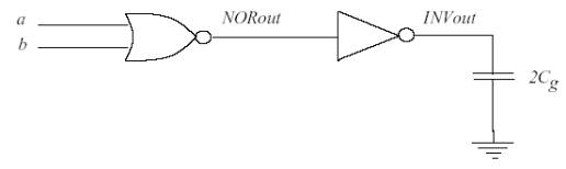
Figure 1: Circuit for Problem 1.
Compute ![]() ,
, ![]() ,
, ![]() ,
, ![]() ,
, ![]() , and
, and ![]() . You may assume that the output load on the inverter is
. You may assume that the output load on the inverter is ![]() and you may ignore
wire lengths in this problem. Use the values below and determine the actual
times in nanoseconds of
and you may ignore
wire lengths in this problem. Use the values below and determine the actual
times in nanoseconds of ![]() followed by
followed by ![]() , and also
, and also ![]() followed by
followed by ![]() . For this problem, assume that the lengths and widths of the
transistors are as follows:
. For this problem, assume that the lengths and widths of the
transistors are as follows:
n-channel
![]() , p-channel
, p-channel ![]()
Use the following values for the transistor gate capacitance and the transistor “on” resistance values to perform an approximate RC analysis as described in class:
nfet
passing ![]() , nfet passing
, nfet passing ![]()
pfet
passing ![]() , pfet passing
, pfet passing ![]()
Gate
Capacitance is![]() for a min size gate.
for a min size gate.
Note that transistors that are “off” are assumed to have infinite resistance, i.e. no leakage.
Standard
size Contacts: ![]() ndiff
ndiff ![]() ,
, ![]() pdiff
pdiff ![]() ,
, ![]() poly
poly ![]() .
.
pdiff
lumped with pchannel ![]() of transistor width.
of transistor width.
ndiff
lumped with nchannel ![]() of transistor width.
of transistor width.
gate
of nfet or pfet ![]() of length where min
width
of length where min
width ![]() .
.
Spice Analysis
For each of the following problems:
1) Use magic to design the circuit, and irsim to simulate the logic.
2) Please hand in a cif2psm l or pplot plot of the circuit, and the results of the irsim simulation.
3) Design an HSPICE experiment file from the descriptions given below.
4) Use ext2spice to build your HSPICE input netlist file. Add the HSPICE transisitor models to the netlist file. Finally, add your HSPICE experiment to the end of the netlist files and save the file with a .sp file extension. Please hand in the final HSPICE .sp input file.
5) Run awaves and then invoke HSPICE to generate output data for plotting the waveforms in the following experiments. Please hand in the awaves plots.
6) There are some demo files in /home/cavallar/demo/hspice/test_demo on Owlnet.
7) See the tutorial handout on the use of HSPICE for a simple string of inverters at http://www.owlnet.rice.edu/~elec422/2001/spice_demo.html
Problem 2: HSPICE Analysis of XOR
Run HSPICE on a static complementary XOR circuit,
such as one designed in HW2. The variable t refers to time in the
description given below.
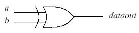
Figure 2: Circuit for Problem 2.
Logic
![]() Volts and logic
Volts and logic ![]() Volts. Mark nodes a, b as inputs and node dataout as
output. Perform the following two transient analysis experiments with HSPICE:
Volts. Mark nodes a, b as inputs and node dataout as
output. Perform the following two transient analysis experiments with HSPICE:
1. Node dataout rises:
At ![]()
At ![]()
2. Node dataout falls:
At ![]()
At![]()
The pulse width needs to be sufficient for the complete transition to occur and settle.
Problem 3: HSPICE Analysis of Pseudo-NMOS Logic
Run HSPICE on the Pseudo-NMOS CMOS circuit shown below. Use a ratio such as the
(4 to 1) ratio used in class to size the p and n channel
transistors. The variable t refers to time in the description given
below.
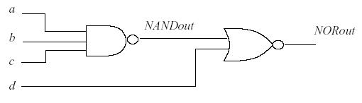
Figure 3: Circuit for Problem 3.
Again, Logic ![]() Volts and logic
Volts and logic ![]() Volts. Mark nodes a, b, c, d as inputs and node out
as output. Perform the following experiments with HSPICE:
Volts. Mark nodes a, b, c, d as inputs and node out
as output. Perform the following experiments with HSPICE:
1. Node NANDout rises and node NORout falls:
At ![]()
At ![]() ,
,
2. Node NANDout falls and node NORout rises:
At ![]()
At ![]()
Again, make sure that the pulse waveforms are of sufficient duration for the complete transitions to occur.
Problem 4: Minimum Density Layer Checking and Corrected CIF FileCreation
This problem is to help you verify the MOSIS minimum density layer rules for your final layout and to help correct final CIF files for Design Rule Errors introduced during the
final CIF creation process.
Please use your layout from the Homework 4 problem where a circuit was placed into the I/O padframe.
Please follow the procedures for creating and adjusting the final CIF file as detailed in the handout on the class web page.
Please follow the note on the minimum density scripts for polysilicon (15%), metal1 (30%), and metal2 (30%) and report back the initial estimates. (Note: metal3 is not subject to density rules for AMI processes which we use.) Modify your layout with additional unconnected sections of these materials (polysilicon, metal1, and metal 2) to achieve the minimums required. CIF the final layout and do a final verification with the irsim simulator to ensure that no damage was done to the actual circuit.
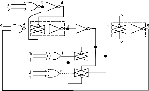
Problem 5: Two-Phase Clocking Timing Analysis
Refer to the circuit diagram below and label the nodes to follow the two-phase timing discipline. Label the following circuit according to the timing discipline discussed by K. Karplus and presented in class. Use labels such as QA, VA, VASB, and so on. Consider Input and Output nodes to only be signals at the external physical boundary of the circuit. You should label the Inputs, a, b, e, h, i, j, k, o, p, with the weakest allowable signal. Based on the timing rules for combinational logic and storage elements, propagate these signals through the interior nodes of the circuit. By doing this, the Outputs should be labeled with the strongest produced signal. The TGATE+INVERTER groups should be considered as dynamic latches (recall the Noice, Mathews, and Newkirk paper), therefore this circuit would be connected to both CLKA and CLKB. Start with signals based on CLKA on the left hand side of the circuit. It is possible that in the circuit as designed below there could be a node or nodes that violate the timing discipline. If this is the case, please try to preserve as much of the circuit as possible and indicate the node or nodes that are in violation. Also, suggest a possible solution to the timing discipline violation.