|
|
|
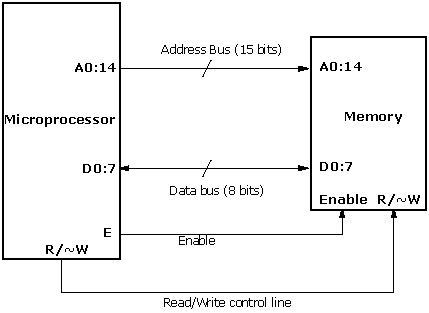
ELEC 201 HardwareThis chapter is partly tutorial and partly technical reference: in additional to documenting the Rice ELEC 201 RoboBoard hardware, it explains the design in a way that assumes minimal background in digital electronics. Additional explanatory material can be found in the Glossary (Appendix B) and in Chapter 12. The information presented here should be considered optional, as it is not strictly necessary to know it to build a robot. Hopefully though, this chapter will satisfy most readers' curiosity about how the ELEC 201 hardware works. The Microprocessor and MemoryAt the most primitive level, a computer consists of a microprocessor, which executes instructions, and a memory, for storing those instructions (as well as other data).
Figure 5.1 is a block diagram of the microprocessor and memory, showing four types of wires that connect the two:
Multiplexing Data and Address Signals
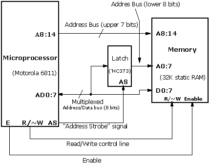
Things are a little more complex with the particular microprocessor that is used in the RoboBoard, the Motorola 68HC11. On the 68HC11, the eight data bus wires take turns acting as address wires as well. When a memory location is accessed (for reading or writing), the data wires act first as address wires, transmitting the eight lower-order bits of the address. Then they function as data wires, either transmitting a data byte (for a write cycle) or receiving a data byte (for a read cycle). All of this happens very fast -- 2 million times per second on the RoboBoard. This kind of split-personality bus is referred to as a multiplexed address and data bus. The memory needs help to deal with a multiplexed address/data bus, provided by an 8-bit latch. This chip (the 74HC373) performs the function of latching, or storing, the 8 address values so that the memory will have the full 15-bit address available for reading or writing data. Figure 5.2 shows how the latch is wired. The upper 7 address bits are normal, and run directly from the microprocessor to the memory. The lower 8 bits are the multiplexed address and data bus. These wires connect to the inputs of the latch and also to the data inputs of the memory. An additional signal, the Address Strobe output of the microprocessor, tells the latch when to grab hold of (latch) the address values from the address/data bus. When the full 15-bit address is available to the memory (7 bits direct from the microprocessor and 8 bits from the latch), the read or write transaction can occur. Because the address/data bus is also wired directly to the memory, data can flow in either direction between the memory and the microprocessor. The entire process -- transmitting the lower address bits, latching these bits, and then the read or write transaction with the memory -- is orchestrated by the microprocessor. The E clock, the Read/Write line, and the Address Strobe line perform in tight synchronization to make sure these operations happen in the correct sequence and within the timing capacities of the actual chip hardware. Memory Mapping
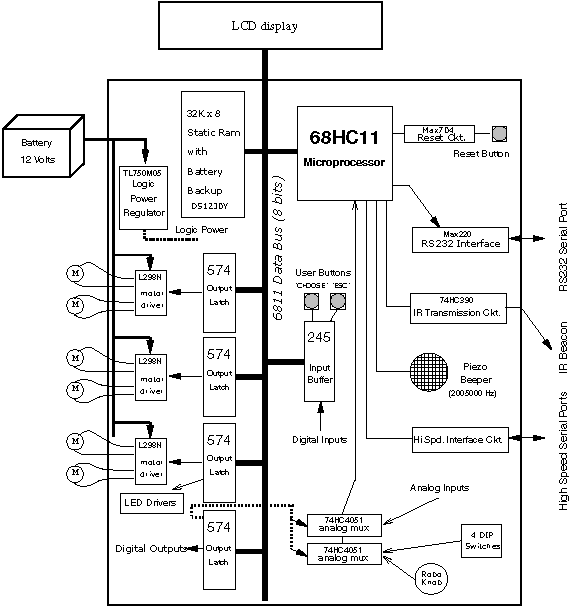
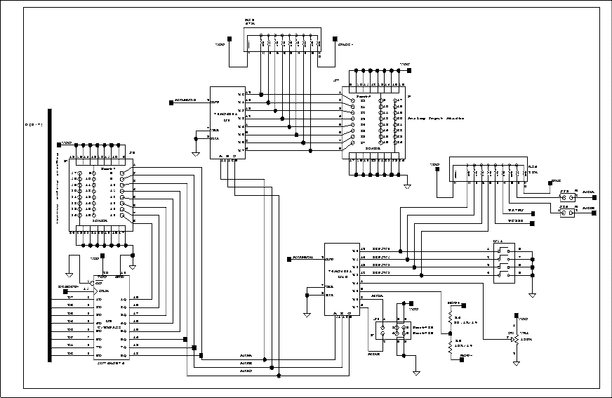
So far we have seen how a memory can be connected to the address space of a microprocessor. In a circuit like the one of the RoboBoard, the microprocessor must interact with other devices besides the memory -- for example, motors and sensors. A typical solution uses 8-bit latches for input and output. These latches are connected to the data bus of the microprocessor so that they appear like a location in memory. Then, the act of reading or writing from one of these memory locations causes data to be read from or written to a latch -- to which the external devices are connected. Figure 5.3 is a block diagram of the ELEC 201 RoboBoard system. Notice that chips marked "574" are connected to the data bus. The '574s have outputs that control the motors (through other chips marked "L298N", which will be discussed later). The digital sensors are driven onto the data bus by a chip marked "245." Another '574 chip is used for eight bits of digital output. These interface chips are used in a technique called memory mapping. The chips are "mapped" to a particular address in the microprocessor's memory. The following discussion will show how both the 32K RAM memory and the digital input and output interface chips share the address space of the microprocessor. Memory-Mapping the RAM
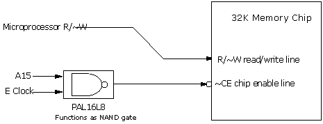
The 68HC11 has a total of 16 address bits, yielding 65536 ("64K") bytes of addressable locations. Half of this space will be taken up by the 32K memory chip (also known as a RAM chip, for "Random Access Memory"). The 68HC11 has a bank of interrupt vectors, which are hardware-defined locations in the address space where the microprocessor expects to find pointers to driver routines. When the microprocessor is reset, it finds the reset vector to determine where it should begin running a program. These vectors are located in the upper 32K of the address space. Thus, it is logical to map the RAM into this upper block, so that the RAM may be used to store these vectors. The technique used to map the memory to the upper 32K block is fairly simple. Whenever the 68HC11's A15 (the highest-order address bit) is logic one, an address in the upper 32K is being selected. The other fifteen address bits (A0 through A14) determine the address within that 32K. A logic gate (actually a portion of a programmable logic device called a "PAL") is used to enable the memory when A15 is logic one and when the E clock is high (since the E clock must control the timing of the enable). Figure 5.4 shows a block diagram of this circuit. Memory chips are part of a class of chips that have active low (sometimes called "active false") enable inputs, meaning that they are enabled when the enable input is logic zero, not logic one. There are two methods for denoting an input that is active low. As shown in Figure 5.4, the chip enable input is shown with connecting to a circle; this circle indicates an active low input. Also, the name for the signal, CE is prefixed with a ~ symbol. The NAND gate shown in Figure 5.4 actually combines two logic functions, a NOT gate (inverter), and an AND gate. The function of the NOT gate is to convert the active-high enable produced by the AND gate into the active low signal required by the ~CE input. Memory-Mapping with the PAL16L8 Chip
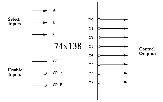
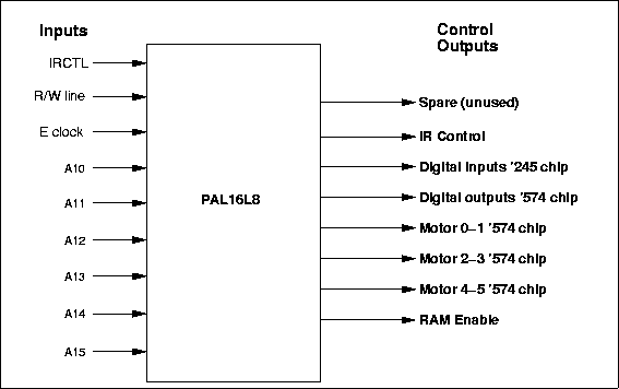
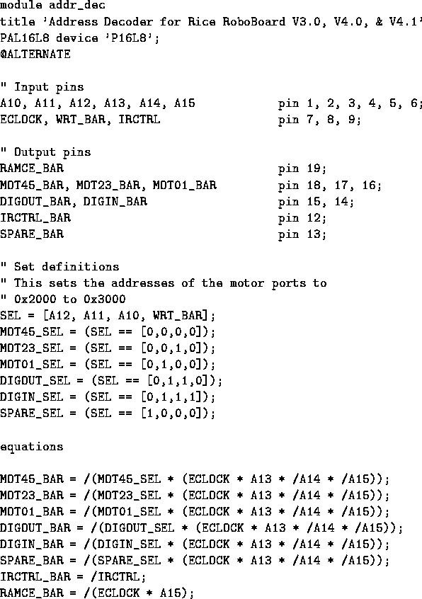
Most computers use a circuit called an address decoder to demultiplex address lines and generate memory-mapped control enables for individual devices. Figure 5.5 shows the logical diagram of a 74x138 demultiplexer, which is commonly used in circuits that map devices onto an address space. This chip is a 3-to-8 decoder: a binary number of three digits (the select inputs) causes one of eight possible outputs to be selected (the control outputs). The chip also has three enable inputs, all of which must be enabled to make the chip become active. Previous versions of the RoboBoard used a 74AC138 for address decoding. Versions 3.0 and later of the RoboBoard implement this functionality using a PAL16L8 programmable logic device. The behavior of this device is controlled by "PAL code", which is shown in Figure 5.7
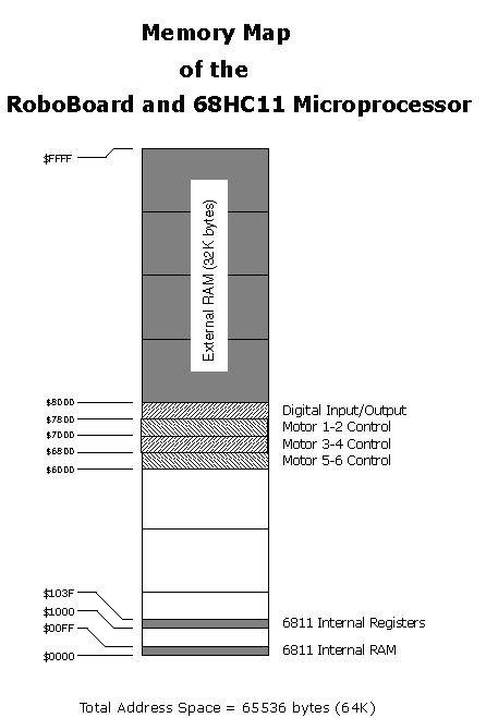
Examining the PAL code (written in a language called "ABEL"), we see that the outputs of the PAL16L8 control the input and output latches shown in the system block diagram. The PAL16L8 determines when these latches are activated, either to read data from the data bus (in the case of the '574 output latch), or to write data onto the data bus (in the case of the '245 input buffer). As determined by the PAL code, the inputs of the PAL16L8 determine when the outputs will become active, and thereby turn on one, and only one, of the control outputs. This is to avoid the possibility that two devices (the RAM and perhaps the '245) would attempt to drive the data bus simultaneously, causing a problematic situation called bus contention. System Memory MapFigure 5.8 summarizes the memory map solution that has been implemented for the ELEC 201 RoboBoard.
The 32K RAM takes up half of the total address space of the microprocessor. As indicated in the map, it is located in the upper 32K of the microprocessor's memory, from addresses $8000 to $FFFF. The digital output and input ports are mapped at location $7800. The three motor control ports are mapped at locations $7000 (motors 1 and 2), $6800 (motors 3 and 4), and $6000 (motors 5 and 6). There is a small area of memory that is internal to the 68HC11 chip itself. This memory consists of 256 bytes located at the start of the address space, from locations $00 to $FF. The 68HC11 also has a bank of 64 internal special function registers, located at addresses $1000 to $103F. These registers control various hardware features of the 68HC11 (the analog inputs and serial communications are two examples).
The remainder of this section presents details on the digital input and output circuit wiring. Digital Inputs
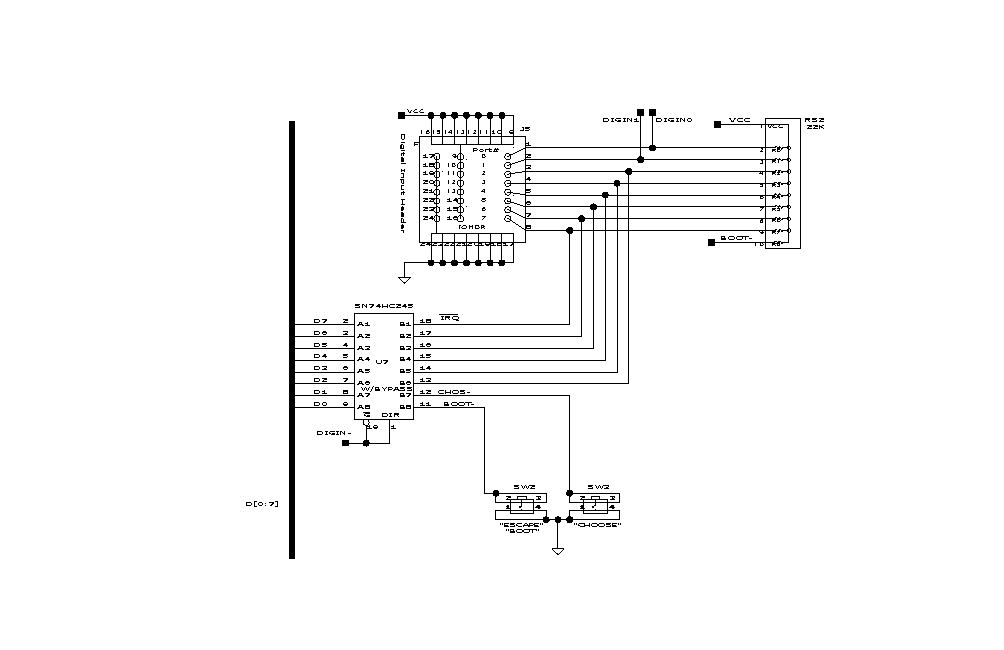
Figure 5.9 shows the digital input circuitry. U7, a 74HC245 chip, is used to buffer an eight-bit word of sensor inputs and drive the 68HC11 data bus with that value when the chip is selected. The '245 is actually a bi-directional buffer or transceiver, but we connect the direction select to the enable so that the '245 can only serve as an input device. The lower two bits of the '245 are connected to the two user buttons (that have been dubbed CHOOSE and ESCAPE). The upper six bits are connected to the digital input header. The lower two bits of the input header are connected to two timer inputs of the 68HC11. These inputs can be used to precisely measure waveforms, or can simply be used for digital input. The library functions written to perform digital inputs insulate the user from the fact that the eight pins on the input header are not mapped contiguously to one location in memory. RS2, a 22K resistor pack, contains pull-up resistors for the inputs of the '245 chip, making the default value of the inputs a logical one. One of the digital inputs (pin 8 of the Digital Input Header) is also tied to one of the 68HC11's external interrupt lines (IRQ, the maskable interrupt). This input is normally pulled high, leaving the interrupt inactive when no input is connected. The default interrupt handler routine simply returns when it is called, so no software modifications need to be made if the input is used as a digital I/O line. However, the simple act of acknowledging and returning from an interrupt takes some time, during which the processor cannot perform other functions. Therefore, frequently changing inputs should not be connected to this digital input. A user defined interrupt routine can be installed if the signal is to be used as an interrupt.
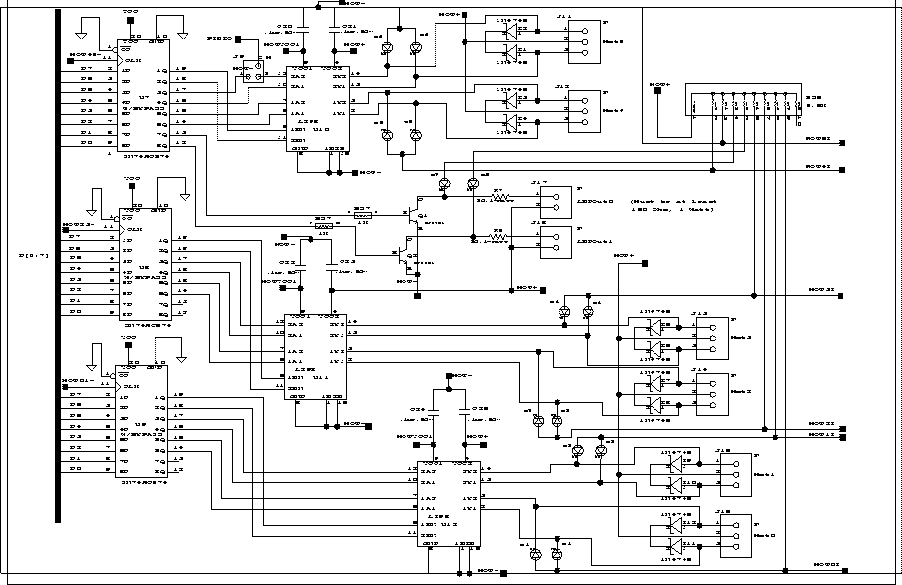
Digital OutputsFigure 5.15 shows the complete schematic for the three '574 output latches controlling the motors. Notice that the data inputs of the '574s are connected to the 68HC11 data bus. The MOT01, MOT23, and MOT45 control signals connect to the clock inputs of the three '574s; when one of these is activated, the corresponding '574 latches the value present on the data bus. The outputs of the '574 connect to the motor driver chips, the circuitry of which is explained in the following section.
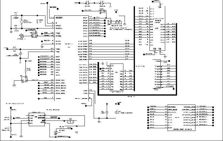
68HC11 and Memory SchematicFigure 5.10 presents the schematic of the 68HC11, memory, address decoding, and supporting main circuitry on the ELEC 201 Processor Board. By the end of this chapter, most of the circuitry depicted here will be explained.
The Motor DriversMotors are high-powered devices in the world of digital electronics. A typical digital output can supply about 10 to 20 milliamperes (mA) of current; a small permanent-magnet motor requires anywhere from 500 to 4000 mA of current. Special circuits are therefore required to drive motors. The H-Bridge Circuit
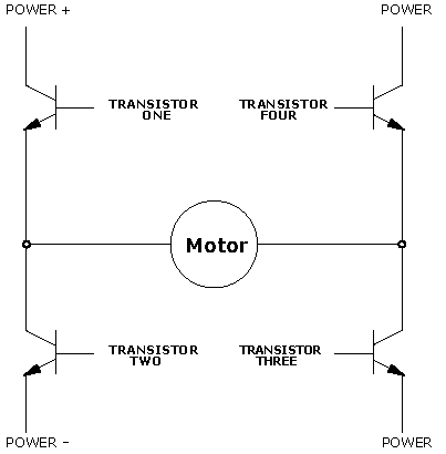
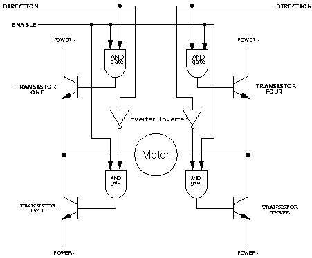
A circuit known as the H-bridge (named for its topological similarity to the letter "H") is commonly used to drive motors. In this circuit (depicted in Figure 5.11), two of four transistors are selectively enabled to control current flow through a motor.
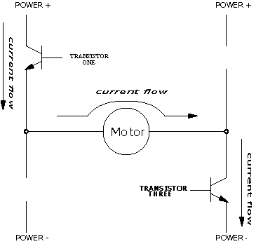
As shown in Figure 5.12, an opposite pair of transistors (Transistor One and Transistor Three) is enabled, allowing current to flow through the motor. The other pair is disabled, and can be thought of as out of the circuit. By determining which pair of transistors is enabled, current can be made to flow in either of the two directions through the motor. Because permanent-magnet motors reverse their direction of turn when the current flow is reversed, this circuit allows bidirectional control of the motor. The H-Bridge with Enable Circuitry
It should be clear that one would never want to enable Transistors One and Two or Transistors Three and Four simultaneously. This would cause current to flow from Power to Power through the transistors, and not the motors, at the maximum current-handling capacity of either the power supply or the transistors. This usually results in failure of the H-Bridge. To prevent the possibility of this failure, enable circuitry as depicted in Figure 5.13 is typically used. In this circuit, the internal inverters ensure that the vertical pairs of transistors are never enabled simultaneously. The Enable input determines whether or not the whole circuit is operational. If this input is false, then none of the transistors are enabled, and the motor is free to coast to a stop. By turning on the Enable input and controlling the two Direction inputs, the motor can be made to turn in either direction. Note that if both direction inputs are the same state (either true or false) and the circuit is enabled, both terminals will be brought to the same voltage (Power or Power, respectively). This operation will actively brake the motor, due to a property of motors known as back emf, in which a motor that is turning generates a voltage counter to its rotation. When both terminals of the motor are brought to the same electrical potential, the back emf causes resistance to the motor's rotation. The SGS Thompson L298N Motor Driver Chip
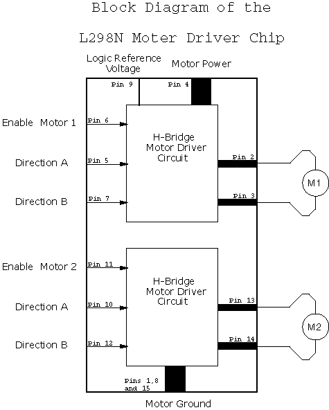
The SGS Thompson L298N 8 motor control chip incorporates two H-bridge motor-driving circuits into a single 15-pin package. Figure 5.14 shows a block diagram of this useful integrated circuit. The schematic of the motor circuit (Figure 5.15) shows how the L298N chips are controlled in the ELEC 201 RoboBoard design. Six bits are used to control two motors. Four of the bits determine the direction of the motors and two bits determine when the motors are on or off. There are three such circuits on the RoboBoard, one for each pair of motors. The remaining two bits of each of the '574 chips are available as extra digital outputs, two of which are connected to transistor drivers. These transistor circuits are well-suited for powering light-load devices, such as LEDs or small lights. The other four outputs are routed to an output header. The speed of a motor may be controlled by pulsing the enable bit of its associated controller chip on and off. This technique, called pulse width modulation, is explained in the chapter on motors.
Power ConsiderationsCurrent Handling and Spike ProtectionThe L298N does not have significant internal protection against spike and other electrical noise. Therefore, diodes and capacitors have been added to the motor control circuitry as shown in Figure 5.15. These diodes and capacitors protect the motor chip and the rest of the circuit from electrical noise (inductive spikes) generated by the motors. The L298N can supply 2000 mA of current per motor. Since the stall current (the current drawn by the motor when the shaft is unable to turn) of the motors used in ELEC 201 is less than 1500 mA, the L298N circuit is adequate for our purposes. Power Supply IsolationElectrical noise generated by motors can be hazardous to a microprocessor circuit even with the use of the diodes. Therefore the motors use separate power circuitry and filtering from the rest of the microprocessor electronics.
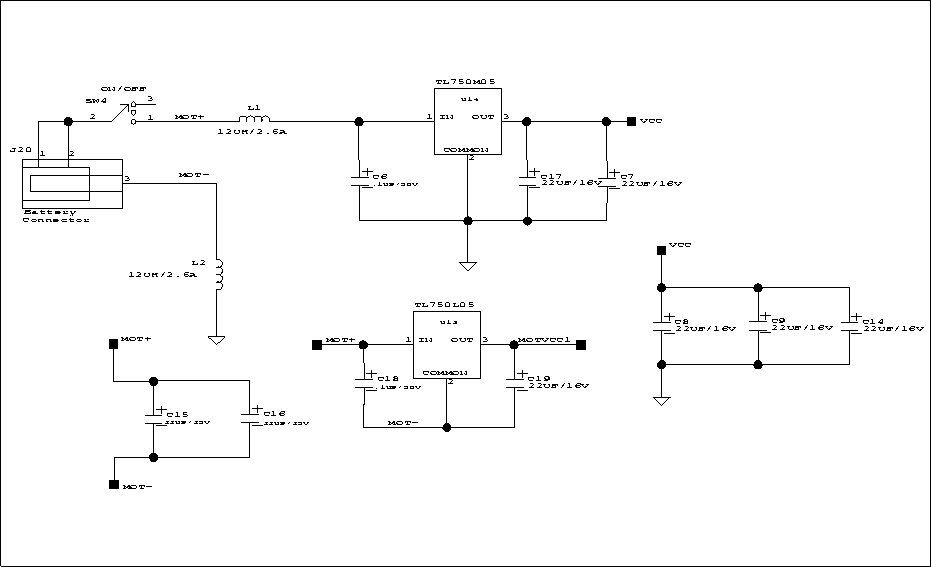
Figure 5.16 shows the power-supply circuitry. Logic power (VCC), the supply voltage for the microprocessor circuitry, is provided by a TL750M05 low-dropout 5-Volt voltage regulator, while Motor power for the motors is supplied directly from the battery. The control circuits of the L298N motor drivers also require a small amount of logic power; this is provided by a separate TL750L05 5-Volt regulator, as shown in Figure 5.16. The motor ground and the logic ground must be kept at the same potential so that the control signals from the '574 chip shown in Figure 5.15 can communicate with the L298N chips. These grounds are kept at the same potential by the inductor L2. Inductor L2 prevents motor current surges from upsetting the microprocessor power supply. The inductors provide reactance (frequency-dependent resistance) to trap electrical noise that might travel from the motors, through the L298N chips, and into the microprocessor circuit.
Analog InputsThe 68HC11 has on-chip circuitry to perform an analog-to-digital signal conversion. In this operation, a voltage from 0 to 5 volts is converted into an 8-bit number (a range of 0 to 255, where zero volts corresponds with 0, and 5 volts with 255). This conversion feature is one of many that make the 68HC11 well-suited for control applications. The 68HC11 has eight of these analog inputs. In the ELEC 201 RoboBoard design, six of these pins are wired to a motor current monitoring circuit, and two of them are wired to analog multiplexors, as described below. Motor Current Monitoring CircuitWhen the L298N chips drive a motor, there is a voltage drop across the transistors that form the H-bridge. The transistor connected to motor ground (0 volt potential) might drive the motor at some voltage between .2 and .8 volts; the transistor connected to the positive terminal of the battery (say it is at 12 volts) might drive the motor between 11.2 and 11.8 volts. The amount of this voltage drop is proportional to the amount of current being supplied by the motor-driving transistor. The greater the supply of current, the greater the voltage drop across the transistor. This somewhat undesirable property of the L298N transistors is exploited to give a crude measurement of the amount of current being driven through the motor. A fundamental property of motors is that, as the amount of work they are performing increases, the amount of current they draw also increases. So the current measurement yields data on how hard the motor is working -- if it is turning freely, if it is stalled, or if it is working somewhere in between. As indicated in Figure 5.15, the voltage feedback point is tapped from the indicator LEDs that are connected to the motor outputs. The voltage across the LEDs will decrease as a result of increased current draw of the motor (and the corresponding decreased performance of the L298Ns). This voltage is fed to a 68HC11 analog input and can be measured by the 68HC11 analog-to-digital conversion hardware. Each of the six motor circuits is wired in this way to a 68HC11 analog input. Analog Input Multiplexing on the RoboBoard
The RoboBoard has two eight-to-one analog multiplexor ICs. These chips (the 74HC4051) have eight inputs and one output; depending on the state of three selector inputs, one of the eight input lines is connected to the output. (Actually, the chip's signals are bidirectional, but for the purpose of this discussion, it is convenient to think of the chip as having eight inputs and one output.) The outputs of the two '4051 chips are wired into the 68HC11 analog inputs. Three signals from the 68HC11 are used to control the multiplexers and select which analog input is mapped to the 68HC11 analog input. These signals are taken from the three low order bits of the digital output port. Figure 5.17 is a schematic of the analog input circuitry on the ELEC 201 RoboBoard. It is easy to see how the use of the analog multiplexor chips greatly expands the analog input capability of the ELEC 201 hardware:
The Serial Line Circuit
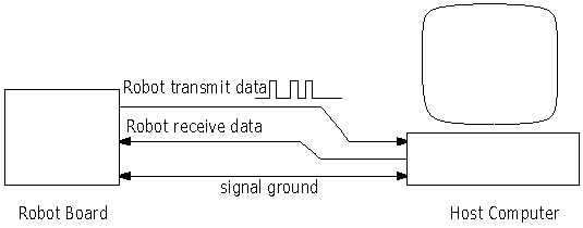
The ELEC 201 Board communicates with a host computer over an RS-232 serial line. "RS-232" refers to a standard protocol for communications over a three-wire system, as depicted in Figure 5.18. Nearly all of today's computers have serial ports that conform to the RS-232 standard.* *The actual RS-232 standard involves quite a few more wires for conveying various status information, but the data itself is transmitted on two uni-directional wires In the RS-232 system, a "logic zero" is indicated by a 10 volt signal with respect to ground, and a "logic one" is indicated by a 10 volt signal. Note that this is different from standard digital logic levels in several ways. Negative voltages are used, higher voltages are used, and negative voltages connote a logic one value. The 68HC11 chip includes circuitry to generate waveforms compatible with the RS-232 systems, but requires external circuitry to convert its own signals, which obey the digital logic norms, to RS-232 signals as described.
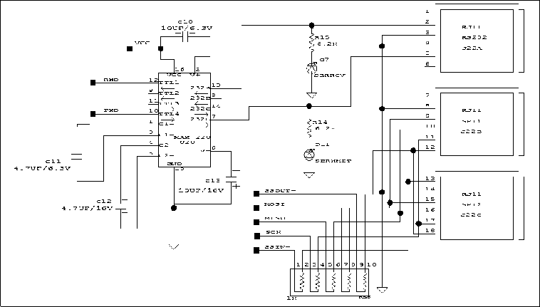
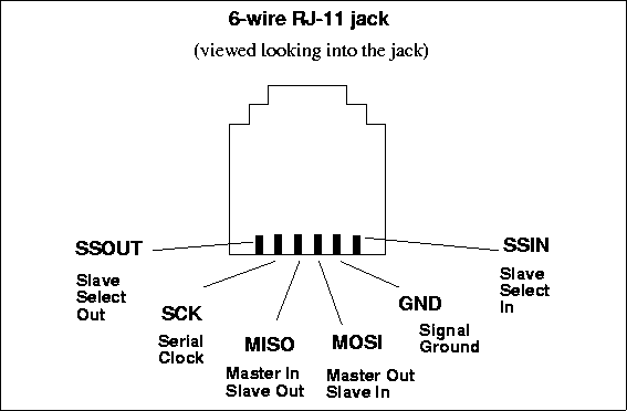
U20, in Figure 5.19, is used to convert between the RS-232 voltage levels, and the digital logic voltage levels used everywhere else on the RoboBoard. This circuit contains two charge pumps to generate the negative voltages that are required. The first is used to double the system voltage of 5 volts to obtain a 10 volt supply that more closely matches the RS-232 standard. The second charge pump inverts this 10 volts to obtain a 10 volt supply. High Speed Serial Peripheral InterfaceThe Serial Peripheral Interface (SPI) circuit is a synchronous serial data link that is standard across many Motorola microprocessors and other peripheral chips. It provides support for a high bandwidth (1 megabit) network connection between CPUs and other devices supporting the SPI. The RoboBoard's two SPI network jacks allow multiple RoboBoards or other SPI devices to be connected using a six-wire RJ-11 (telephone jack) connection. This six-wire RJ-11 interface is downward compatible with the four-wire SPI interface found on the M.I.T. "Mini Board". The RoboBoard uses a particular configuration of the SPI system that requires a minimum of external hardware support. Multiple RoboBoards may be networked with no additional components other than the cabling itself. A brief review of the SPI system follows, along with a discussion of the particular configuration of the SPI on the RoboBoard. Further details can be found in the Motorola M68HC11 Reference Manual. Introduction to the SPIThe Serial Peripheral Interface is essentially a shift register that serially transmits data bits to other SPIs. During a data transfer, one SPI system acts as the "master" that controls the data flow, while the other system acts as the "slave" that has data shifted into and out of it by the master. Different CPUs can take turns being master, and one master may simultaneously shift data into multiple slaves. However, only one slave may drive its output to write data back to the master at any given time. The basic SPI interface consists of two data lines and two control lines:
RoboBoard SPI Configuration
The RoboBoard uses a six-wire SPI connection that carries the MOSI, MISO, SCK, signal ground, and two lines that support the Slave Select function (see Figure 5.20). Slave Select Out is a digital output that is driven by bit 5 of Port A. Slave Select In to the 68HC11 is configured by J3 on the RoboBoard. If pins 1 and 3 are connected, Slave Select In is tied low (this is the Mini Board compatible configuration), if pins 2 and 3 are connected, Slave Select In is tied high, and if no jumper is installed in J3, Slave Select In will be at whatever level is present on the RJ-11 pin. In the Mini Board compatible configuration, software protocols must be used to enable the activity of the SPI slave. In the default configuration (no jumper in J3), multiple RoboBoards can be arranged in a "ring" topology, with mastership being passed around the ring by each RoboBoard controlling the Slave Select In of the downstream board. To connect the SPI circuits of multiple RoboBoards, each respective line of each RoboBoard can be tied together: MOSI to MOSI, MISO to MISO, etc. To make this happen, the connecting RJ-11 cables must have half-twists in them. This configuration works because of the bi-directionality of each of the control lines. When a given SPI circuit is the master, it transmits on its MOSI line while slaves receive on their MOSI lines. Likewise a slave transmits on its MISO line and the master receives on its MISO line. The SCK line also is automatically configured properly (it is an output for the master and an input for the slave).
Suggested ProtocolsTwo sample protocols are presented. The former, a single master protocol, would be significantly easier to implement than the latter, a multiple master protocol.
Non-Volatile Static RAMThe static RAM used in the ELEC 201 board is a special device, manufactured by Dallas Semiconductor, that contains a 32K x 8 RAM, a small battery, and some circuitry that switches between normal and battery back-up power under controlled conditions. Having a battery-backed static memory greatly increases the usability of the ELEC 201 board, since a robot can simply be turned on and operated immediately, without having to be connected to a computer first. The Infrared Transmission Circuit
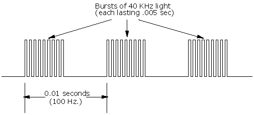
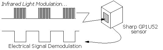
The Sharp GP1U52 sensor and others like it, commonly used in TVs, VCRs, and other devices controlled by infrared, is sensitive to modulated infrared light. It detects the presence of infrared light that is blinking on and off at a particular rate. The GP1U52 sensor is tuned to 40,000 Hertz (40 KHz). In TV remote applications, a data stream is then generated around the 40 KHz carrier frequency. The signal consists of bursts and gaps of the 40 KHz transmissions.
For the ELEC 201 application, the 40 KHz carrier is used to transmit a square wave of relatively low frequency (100 or 125 Hz), as shown in Figure 5.21. When the Sharp IR sensor decodes this signal, it removes the 40 KHz carrier, yielding a copy of the square wave that was originally transmitted (Figure 5.22). The ELEC 201 system software continuously checks the Sharp sensors for square waves of the specified frequency. The software actually locks on to the square wave when it is present and then counts the number of consecutive cycles that have been detected.
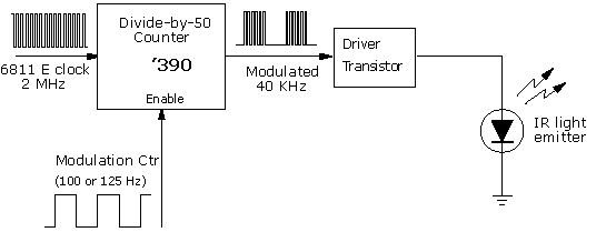
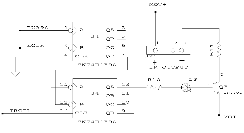
A special circuit is used to generate infrared emissions modulated at the 40 KHz frequency. A block diagram of this circuit is shown in Figure 5.23. The diagram shows that the '390 chip, wired in a divide-by-fifty configuration, is used to generate a 40 KHz signal from the 68HC11 E clock, a 2 MHz signal. In actuality, the '390 chip contains two decade counters. Each these consists of a separate divide-by-five counter and a flip-flop (a divide-by-two device). The '390 is wired in the divide-by-fifty function by ganging two of the divide-by-five counters and one of the flip-flops. The IR control signal is wired to the clear input of the '390 chip; when this signal is true, the counters will reset and will be prevented from counting. By modulating this signal, the 68HC11 can generate the low-frequency square wave that ends up being transmitted to the Sharp sensor. Figure 5.24 shows the full circuit schematic for the IR subsystem. The 2N4401 transistor is used to drive the infrared LEDs.
The IR Beacon
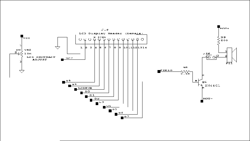
The IR beacon is like the remote control for your TV. The IR beacon emits a modulated signal containing information which is received and interpreted by the IR sensor and the RoboBoard. This process is much like the transmission that occurs when you press a button on the remote control. The IR beacon for ELEC 201, however, has two design challenges to tackle. Figure 5.25 shows the schematic for the IR beacon. The IR beacon must produce a signal with the maximum possible strength so that it can be easily detected, and detected at reasonable distances. Optical power output and current have a linear relationship, so in order to increase the signal strength, current must be increased. Unfortunately, increasing the current supplied to the IR board shortens the battery's life. In order to minimize the current, the IR LEDs are all wired in series. To change channels one would point the remote at the TV and press a button. The robots, though, must broadcast their signal in every direction. Again, there is a tradeoff that must be optimized. Infrared LEDs have the property that as the viewing angle increases, the radiant intensity decreases. The Sharp GL537 LEDs used on the 1999 IR board provide the best compromise between power and viewing angle and are used in commercial remote control applications. The IR board also has two indicator lights so that you can make sure everything is working. The red LED labeled IR XMIT on the RoboBoard lights up when the RoboBoard is attempting to transmit a signal. The red LED on the IR board lights up when all the IR LEDs are transmitting. The LCD DisplayJ19 (in Figure 5.26) is a fourteen pin header designed to be compatible with a 14-pin standard LCD bus. A variety of character-based LCD devices with different screen sizes use this standard bus. The LCD bus standard is fairly simple, consisting of the following signals:
In fact, reading and writing data to an LCD is much like reading and writing data to latches or to memory. There is one problem, however: LCDs only work at data transfer rates up to 1 MHz. The 68HC11 on the ELEC 201 RoboBoard operates at 2 MHz -- too fast for most LCDs. One straight-forward solution to the speed problem would be to use a '574-type latch between the 68HC11 and the LCD. The '574 could be written to at the full bus rate of the 68HC11; its outputs would drive the data bus of the LCD. A separate signal could be used to toggle the LCD's clock line, causing it to latch the data that had been written to the '574. This solution assumes that one does not need to read status data back from the LCD. An unconventional, zero-additional-hardware solution has been implemented in the ELEC 201 system, which takes advantage of an obscure feature of the 68HC11 microprocessor. The 68HC11 has two main operating modes, known as single chip mode and expanded multiplexed mode. The discussion of memory read and write cycles that has been presented in this chapter has been based on the expanded multiplexed mode, which is the 68HC11 mode that is used when external memory is part of the 68HC11 circuit. When the 68HC11 is operated in single-chip mode, the upper-eight-bit address bus and multiplexed address/data bus become general purpose inputs and outputs of the 68HC11, controllable by system software. Thus, in single-chip mode, the 68HC11 could communicate with the LCD with a software driver, rather than the too-fast hardware communication. There is a problem with this, however: when the 68HC11 is placed into single-chip mode, it can no longer execute a program from its external RAM. In fact, as far as the 68HC11 is concerned, there is no external memory. Fortunately, the 68HC11 has 256 bytes of internal RAM, from which it can execute a program when in single-chip mode. Thus, a software driver could execute out of internal RAM, perform a transaction with the LCD, and then switch back to expanded-multiplexed mode and return control to the main program in external memory. The obscure feature mentioned is not the fact that the 68HC11 has both of these modes, but the idea of dynamically switching between them. Here is the solution that has been implemented:
The actual LCD driver routine buffers characters to be printed to the LCD; one thousand times per second, an interrupt routine calls the internal memory driver as described, writing a single character to the LCD. The whole process operates transparently to the ELEC 201 system user.
|