Overall Diagram
Sub-Diagrams
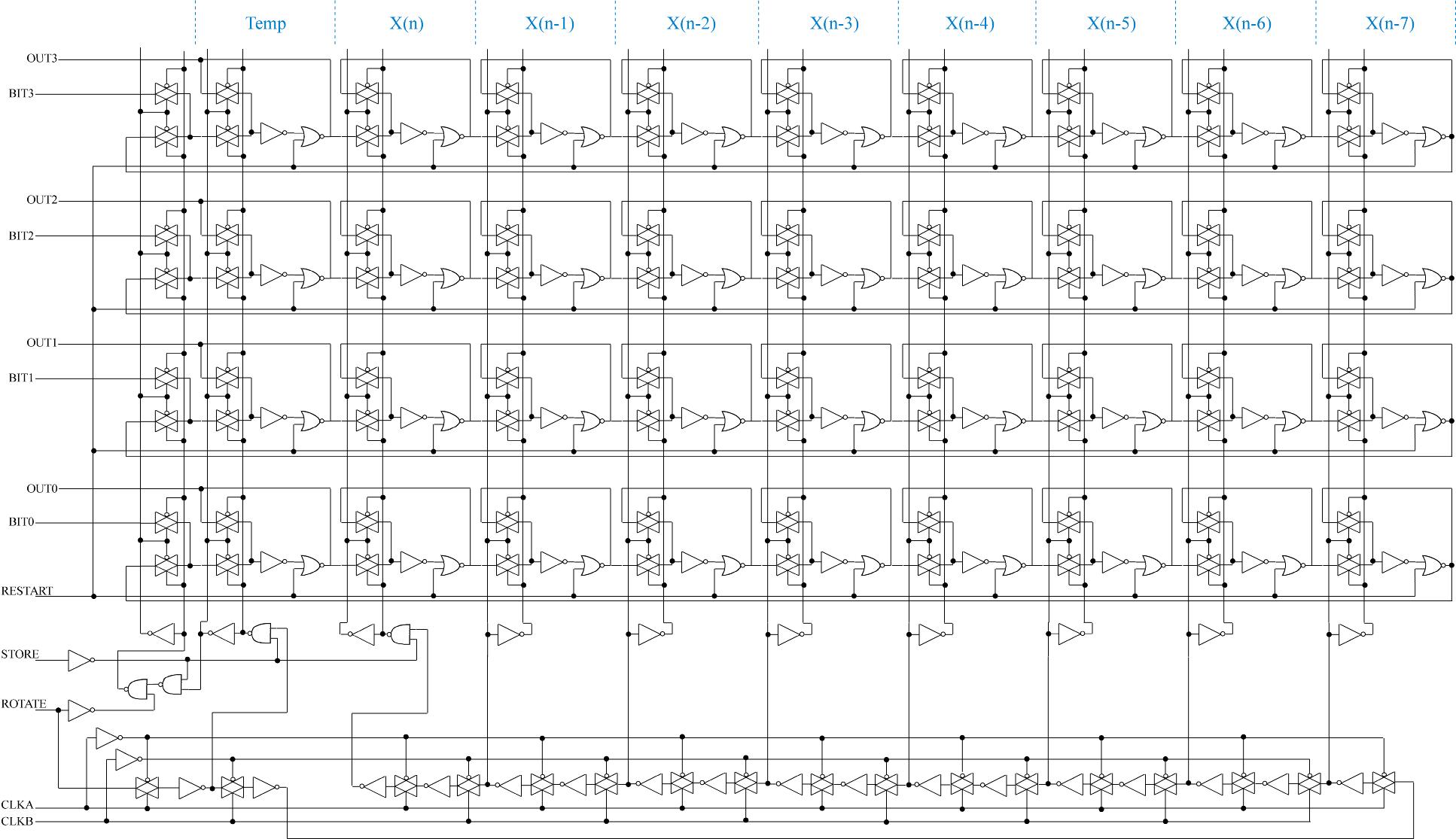
8-bit Rotate Stack (NOTE: only 4 bits are shown in order to conserve space)
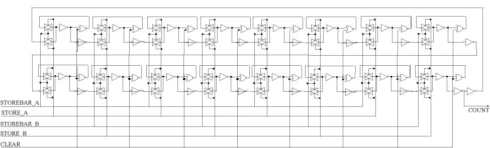
The diagram below presents a high-level representation of the entire system. The inputs to the system are coming in on the left and the outputs are leaving on the right. The desired input D comes into an 8-bit latch and the X input comes into an 8-bit stack. Each are sampled at a certain rate by an A/D converter and after each iteration of the whole system these samples are stored. There are two phases that are completed on each iteration: calculating the error and updating the filter tap weights. Both of these phases are described in more detail w/ timing in System Timing. There are five MUXs in the system that are used primarily to choose between different inputs to both the multiplier and adder in order to reuse them since we do not have space on our chip to have multiple functional units. There is also a second stack for storing each of the filter tap weights in the lower left hand corner of the diagram. The two latches that feed back from the output of the adder to one of its inputs are used for accumulation and the latch at the far right is used for storing the final error once it is calculated. The multiplier is shown in the middle, there are two things to notice about the multiplier. First, since it is an 8-bit multiplier the output of the multiplier is 16 bits. This is true in our system, however a 16-bit bus would have been too large to fit on our chip so we throw away 4 of the outputs and keep only 12 bits. From our MatLab simulations, we determined that 12 bits would be sufficient to represent the values multiplied. In addition, the multiplexer at the output of the multiplier is used for choosing the normal 12 bit output or the 12 bit output right shifted by 5. This "right shifted" output is only used when we are calculating the new value of the weights for the updating phase and was necessary to keep the value of the weights normalized. This is explained further in the LMS Algorithm Section. One other thing to note is the output of the adder. Since the width of our inputs and weights are only 8 bits (again, for space purposes), the output of the adder has to be truncated down from 12 to 8 bits.
![]()
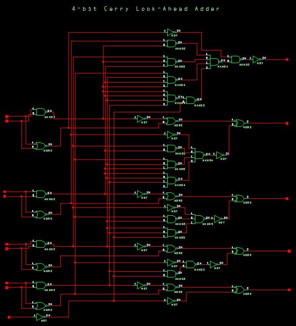
The diagram below represents our 4-bit carry-look ahead adder circuit. Essentially, the inputs A and B come in on the left as well as the carry at the far bottom left and the four sum outputs are on the right as well as the carry out at the top right. Notice, as explained earlier, that the complexity of the logic increases with each bit and the carry generation circuit at the top requires a 5-input NAND gate to generate the carry output.
![]()
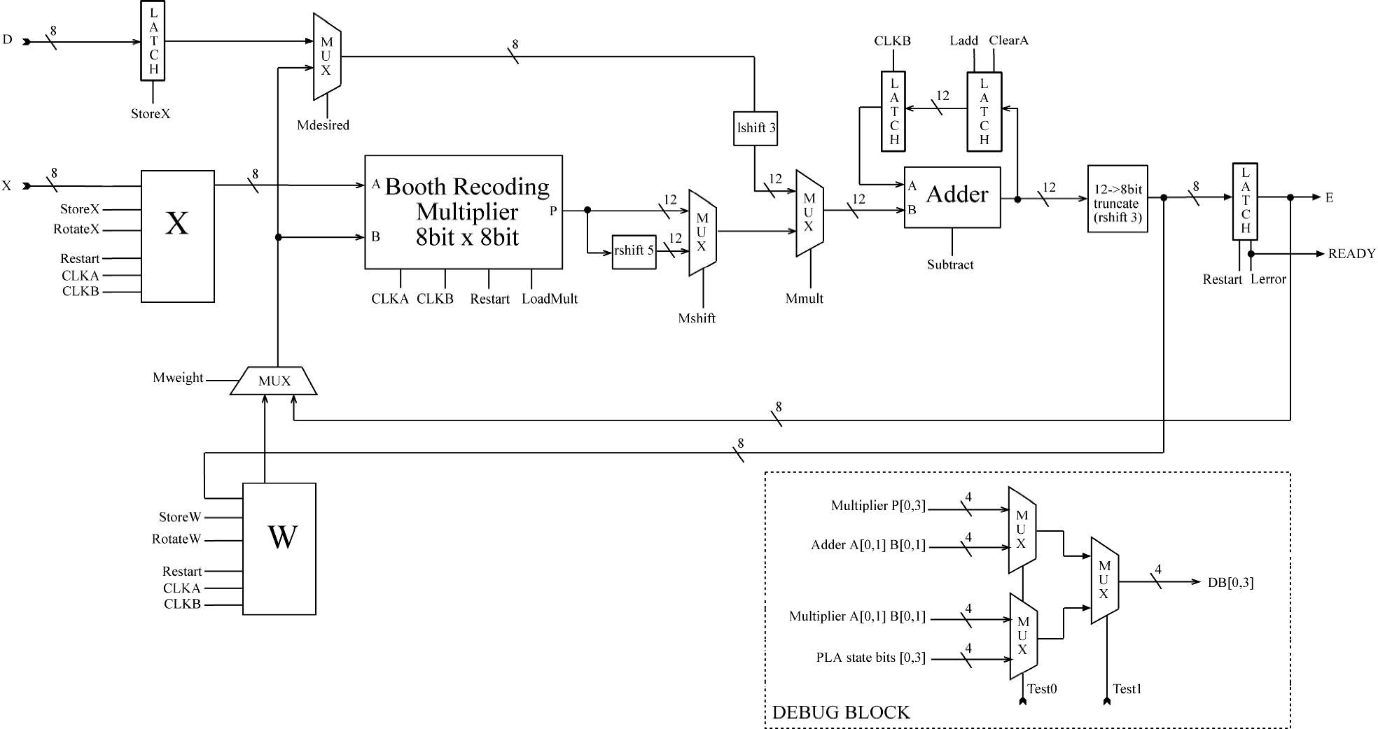
Radix-4 Booth Recoding Multiplier
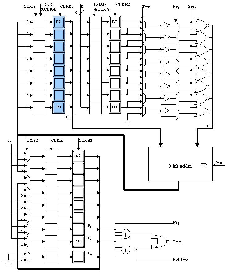
The logic diagram for the Radix-4 booth recoder is shown below. The first thing to note about this circuit is the fact that it is always producing an output since all of the latches are controlled by CLKA and CLKB2 and it only requires one control signal to set the input. The multiplier works as follows. Upon the PLA sending a load signal to the multiplier, the A and B inputs are latched on CLKA and the upper 8 bits of the P register (at the top left) are cleared. In the case of latching A, the load signal is used to choose between the feedback from the 9-bit adder and the external A input value to be multiplied so when load is high the external input is chosen. CLKB2 is the CLKB signal divided by 2, in other words it is goes high only half the time CLKB goes high. This is because we only need to latch the product every other cycle. After A and P are latched on CLKA, they are shifted into the next set of latches on CLKB2 (the multiplier requires that you only start a multiply on CLKB2 cycles so that the input is immediately shifted in). The two LSBs of the product and the last bit shifted out (initially zero) are sent through some logic to create the control signals for determining which value of B to add to the product (0, B, -B, 2B, -2B). The Two control signal controls choosing between B or 2B (simply shifting all the bits to the left). The Neg control signal chooses between adding a negative or positive value of B (NOTE that the negation of B is obtained by inverting each bit and also sending the Neg signal into the carry in of the adder to obtain the 2's complement). The Zero control signal chooses between adding the value of B obtained thus far or 0. So after the first cycle a second cycle is left for these signals to obtain the correct input of B for the adder and for the adder output to stabilize. The output of the adder is fed back into the product register (NOTE that the load signal must be zero during this time because this will allow the output of the adder to be fed back into the adder and shifted by 2 using the MUXs. This completes one iteration of the multiplier, it takes four such iterations to generate the final output of a multiply operation. In all, the multiplier takes 10 clock cycles.
![]()
![]()
8-bit Rotate Stack (only 4 bits shown)
The logic diagram for the Rotate Stack is shown below. Note that this only comprises 4 bits of the stack, each row in the circuit must be duplicated four more times to obtain the 8-bit stack we are using.
![]()
The logic diagram for the ring counter is shown below. It is essentially a ring oscillator whose COUNT value changes every 8 cycles of both the STORE_A and STORE_B qualified signals. It is constructed with 16 latches in series, alternating the STORE_A and STORE_B signals to control them. The output of the final latch is inverted and sent back to the input of the first latch. The CLEAR signal is used to clear all of the latches to 0 in order to start a count. Thus, the inverter will invert the input of the first latch to 1 and it will take 8 COUNT cycles for the 1 to reach the COUNT output at the input of the inverter. We use two counters in our system in conjunction with the PLA. The first is used to count the number of clock cycles for the multiplier and STORE_A and STORE_B are simply the CLKA and CLKB signals. The second is used to count the number of multiply operations that have been performed, thus it must be controlled using two signals from the PLA in order to increment the count every time a multiply operation is started. Since the two signals cannot be high simultaneously and it is not necessary for the count to be immediately updated in the same cycle, the PLA sends the two signals on two different cycles.
![]()