
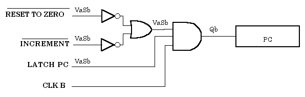
FUNCTIONAL DESCRIPTION
The program counter, PC, is a
special-purpose register that is used by the processor to hold
the address of the next instruction to be executed. The PLA automatically
updates the PC to point to the next instruction during the op-code
decode cycle. By coordinating with other hardware, in addition
to the PLA, the PC is automatically incremented as each instruction
is executed. The PC can also have an address dictated to it via
the 'BRANCH' instruction.
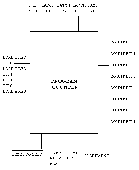
Found in figure 1 below is the
functional level block diagram of the PC designed for this microprocessor.
The PC possesses the following attributes: outputs an 8-bit address,
resets to zero, can be loaded with any 1 of the possible 256 addresses
and produces an overflow flag if the counter exceeds 256. When
the device is reset, via an external pin, the '/RESET TO ZERO'
pin is pulled low by the PLA resulting in the PC being set to
00h. The PC is incremented by the PLA by pulling the '/INCREMENT'
pin low for 1 clock cycle. If the PC is incremented past its 256
word address reach the 'OVER FLOW FLAG' pin will be driven high.
The PC can be forced to a specified value with the use of the
'BRANCH' command. When the PLA decodes a 'BRANCH', the PC will
latch in the contents of the next 2 addresses. The processor then
shifts the concatenated 8-bit address into the PC.
Figure 1
REGISTER TRANSFER LEVEL
DESCRIPTION
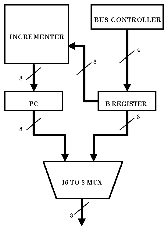
As shown in figure 2, the PC has
several components that aid in the task of providing the address
of the next instruction. During a reset, the PLA resets the incrementer
to 00h and then latches the output of the incrementer into the
PC. The value contained in the PC is then driven out through the
multiplexer by the PLA selecting the PC data path. For each time
the PLA implements an increment PC, the incrementer is advanced
by 1 and then shifted into the PC register. The value contained
within the PC is then selected to pass through the multiplexer
whose output is directly tied to the address pins. When the PLA
decodes a 'BRANCH' op code, the contents of the next 2 addresses
are shifted into the B register via the data bus controller. Once
the branch address is shifted into the B register the value is
then loaded into the incrementer. The PLA then proceeds to pass
the contents of the B register through the multiplexer to the
address pins. On the next increment PC, the value that was shifted
into the incrementer from the B register is incremented, shifted
into the PC and passed through the multiplexer.
Figure 2
GATE LEVEL DESCRIPTION
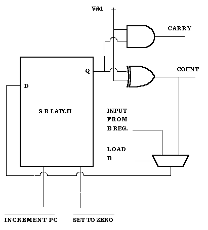
Incrementer
The 8-bit incrementer is base
on the circuit displayed in figure 3. The incrementer circuit
has the ability to be reset to 0 and to be incremented by 1. The
8-bit incrementer is constructed by routing the carry signal around
to the input of the AND gate of the next incrementer circuit.
The LSB of the incrementer has the input of the AND gate tied
to Vdd. The 'COUNT' signal of the MSB is used as the 'OVER FLOW
FLAG', signifying that the increment has exceeded its 8-bit limit.
Figure 3
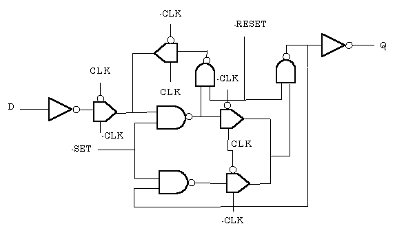
S-R Latch
The incrementer circuit uses an
S-R latch to provide the ability to reset the incrementer to 00h
and to latch the current address. The gate level schematic of
the S-R latch used in the incrementer design is shown below in
figure 4. The 'CLK' and '-CLK' signals are tied to '/INCREMENT
PC' and 'INCREMENT PC' respectively. In addition, the '-RESET'
is mapped to '/SET TO ZERO' in the 8-bit increment design. In
the silicon implementation of the 8-bit incrementer, the 'CLK'
and '-CLK' signals were heavily buffered to ensure that rising
and falling edges of these signal contained very little skew.
In addition, the '-SET' signal was tied to Vdd since it had no
application in this design.
Figure 4
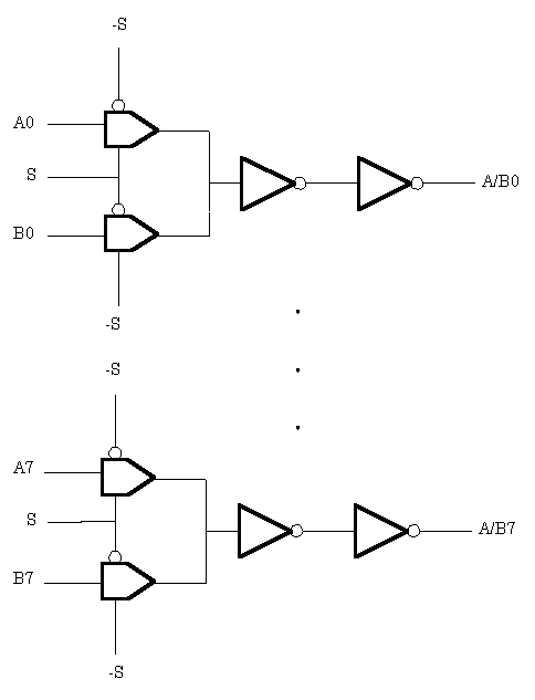
Multiplexer
The multiplexer used in the PC
design is used to pass either the PC register or the B register.
The 16-to-8 multiplexer was constructed by concatenating 8 2-to-1
multiplexer. As shown in figure 5 the 2-to-1 multiplexer is buffered
by implementing 2 inverters at the output of the multiplexer.
The final design of the 16-to-8 multiplexer is designed such that
only 1 control signal is supplied by the PLA to either pass the
PC register or the B register.
Figure 5
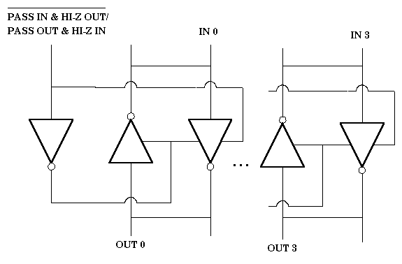
Bidirectional Bus Controller
The bidirection bus controller
is used to allow the 4-bit addresses to be latched from the data
bus into the B register. When the PLA is executing a 'BRANCH'
instruction the address of the location to be branch to is latch
into the B register. When the PLA is not latching a value into
the B register the bidirection bus controller is put into hi-z
state. The hi-z state is necessary to ensure that the data bus
is not heavily loaded when the B register is not latching data
in.
Figure 6
SILICON LEVEL DESCRIPTION
The silicon level implementation
of the PC and associated hardware was completed with minimization
of area as the primary focus. Of secondary importance was speed
and the ability to easily integrate with other blocks of the CPU.
Great care was taken in the layout of the incrementer, multiplexer,
and bus controller to ensure that area consumption was at a minimum.
Examples of good layout techniques that were implemented in the
design of the PC are as follows: overlay of power and ground supplies,
weaving of buses, use of poly for local connections and all ports
brought out to periphery of components. Each individual component
was thoroughly tested from the transistor level up to the functional
level. It was found through testing that the performance of the
8-bit incrementer could be enhanced by providing a heavily buffered
'/INCREMENT PC' signal from the PLA. In the final analysis of
the PC and associated hardware it was found to be fully functional
and performed to specifications.
PC TIMING CIRCUITRY
Shown in figure 7 below is the
required timing circuitry used to coordinate between the incrementer
and the PC register. The timing circuitry ensures that the PC
will latch the value driven by the incrementer one-half cycle
after the incrementer has been reset to zero or incremented.
Figure 7
| Back to the front page | On to next page... |