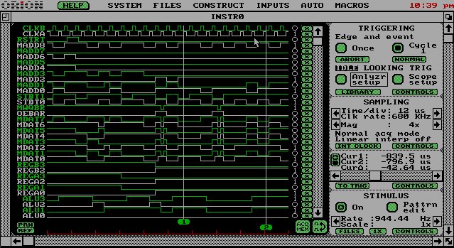
This file is designed to verify that mem2reg passes all logic values on all bus lines correctly. Note that we already know that Mem2RegMux passes the correct values when its control signal is 0 through our testing in regpaths.
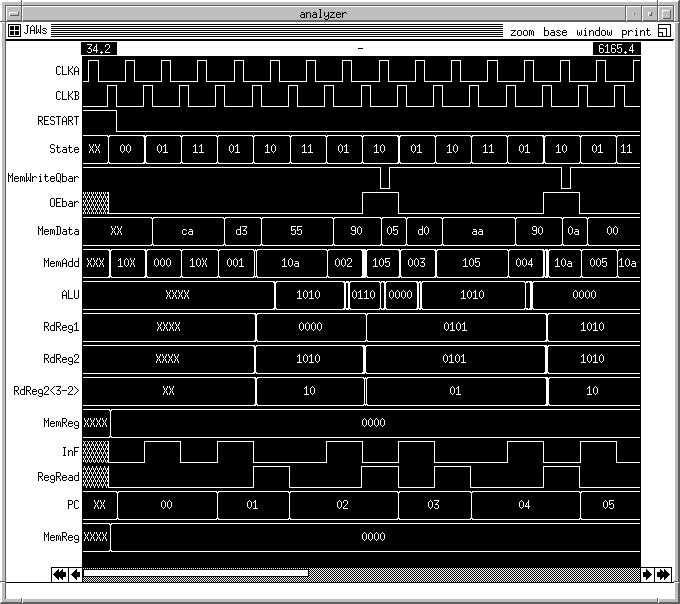
We discovered a problem in our initial test vectors. We planned to use the following program.
Instruction Sequence:
Restart of the chip ...
LDI1010
LW0011 mem data = 01010101
SW0000
LW0000 mem data = 10101010
SW0000
NOOP
But we discovered that it requires writing to MemAdd 105, then reading a different value from the same address. This slipped through last semester, since we were providing the memory responses ourselves. But since we were using the SRAM, we could not accomplish this. We extracted what useful information we could from this test (with Chip 5 only), but we have confidence in Mem2Reg from its success in all of our other tests.
Chip 5 performed as we would expect with properly functioning SRAM, although this result does not agree with the irsim results shown (from last semester). Chip 5 does indeed read back the same value that it wrote to memory.
| SRAM Test

logfile cpu.log

clock Vdd      1 1 1 1
clock CLKA     0 1 0 0
clock CLKB     0 0 0 1

| pin vectors
vector MemData MemData7 MemData6 MemData5 MemData4 MemData3 MemData2 MemData1 MemData0
vector iMemData iMemData7 iMemData6 iMemData5 iMemData4 iMemData3 iMemData2 iMemData1 iMemData0
vector MemAdd  MemAdd8 MemAdd7 MemAdd6 MemAdd5 MemAdd4 MemAdd3 MemAdd2 MemAdd1 MemAdd0
vector iMemAdd  iMemAdd8 iMemAdd7 iMemAdd6 iMemAdd5 iMemAdd4 iMemAdd3 iMemAdd2 iMemAdd1 iMemAdd0
vector State   StBit0 StBit1
vector RdReg1 RegA3 RegA2 RegA1 RegA0
vector RdReg232 RegB3 RegB2
vector ALU ALU3 ALU2 ALU1 ALU0

| pin ana's

ana CLKA CLKB Restart MemAdd  State MemWriteQbar OEbar MemData RdReg232
ana RdReg1 ALU Vdd
ana Trigger

ana ILOAD WE_L iMemData
|ana iMemAdd  <- not enough room on analyzer pins


V RESTART   0
V iMemAdd  000000000 000000000  000000000 000000001 000000001 000000001 000000010 000000010 000000010 000000011 000000011 000000011
V ILOAD     0
V ILOAD_bar 1
V WE_L      1 0 1  1 0 1  1 0 1  1 0 1
V iMemData 11001010 11001010 11001010 11010011 11010011 11010011 10010000 10010000 10010000 11010000 11010000 11010000
R
V RESTART   0 0 0 0 0 0 0 0 0 0 0 0 0 0 0 1 0 0
V ILOAD     0 0 0 0 0 0 0 0 0 0 0 0 0 1 1 1 1 1
V ILOAD_bar 1 1 1 1 1 1 1 1 1 1 1 1 1 0 0 0 0 0
V WE_L      1 0 1 1 0 1 1 0 1 1 0 1 1 1 1 1 1 1
V iMemAdd  000000100 000000100  000000100 000000101 000000101 000000101 100000101 100000101 100000101 100001010 100001010 100001010 111111111 111111111 111111111 111111111 111111111 111111111
V iMemData 10010000 10010000 10010000 00000000 00000000 00000000 10101010 10101010 10101010 01010101 01010101 01010101 11111111 11111111 11111111  11111111  11111111  11111111
R

V ILOAD     1 1 1 1 1 1 1 1 1 1 1 1 1 1 1 1 1 1 1 1 1 1 1 1 1 1 1 1 1 1 1 1 1 1 1 1 1 1 1 1 1 1 1 1 1 1 1 1 1 1 1 1 1 1 1 1 1 1 1 1 1 1 1 1 1 1 1 1 1 1 1 1 1 1 1
V ILOAD_bar 0
V WE_L    1
V iMemAdd  111111111
V iMemData 11111111
V RESTART 0
R