Test Vector Results / OMNILAB Analysis:
-
Paths Verified
- Program Counter increment or branch
- Register Paths (write back, address lines, and reading)
- Memory Address InF Mux path
- Mem2Reg Mux path
Functionality Tests
Programs
The following table reflects the average impedance between any 2 of the three Vdd (or GND) pins,
as well as the Vdd-GND isolation.
The failure of Chip 3's Vdd-GND isolation is discussed below.
The following table reflects the results obtained from our test vectors. Note that a
PASS represents complete functionality. Chip 3 was
not tested because of its failure of the Vdd-GND test.
Chips 2, 4, and 5 exhibited identical results on all tests, so we have
displayed one screen capture for each test vector result.
CHIP 3:
CHIP 1:
The failures are shown below:
When we observed the chip after taking off the lid, we noticed a broken wire connecting the
CPU padframe to the IC case. This wire was on pin 16, which was bit #4 of our MemData bus. The
broken wire is visible on our chip photo in the top right corner.
It is possible
that this pin floated low in the add1path test, since all instructions have a "0" for that bit.
In the insfunc test, some instructions require a "1" for that bit. We note changing register values
in the failed insfunc test, which were likely caused by glitches in the MemData4 signal. We moved on to SRAM testing after
that, and no further tests were conducted on Chip #1.
With the SRAM connected to our chip, we predicted a maximum speed of 4.55 MHz.
This figure was based on the 55ns minumum write pulse width, as specified on the SRAM data sheet.
Using our multiply and memtest tests, we
were able to increase the OMNILAB clock speed up to 17 MHZ (effective chip speed 4.25 MHz), and
still observe complete functionality. We feel these give a good prediction of maximum clock
speed because the multiply test requires a large number of operations, and the memtest test
verifies SRAM read/write functionality.
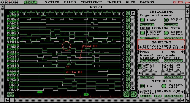
The following figure shows multiply at 4.25 MHz. Note the correct result being written to memory.
The PC is also correct, and register values are as predicted.
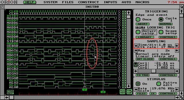
Now, we look at memtest operating at 17 MHz. We verify that the correct value is written to memory,
and in the following instruction, that it is properly read back from memory. Oddly, we do not observe
a pulse in the write cycle on MemWriteQBar, but we can verify that it properly wrote to memory
since we read in the correct value on the next cycle. We conclude that this pulse was too narrow
for OMNILAB to display.
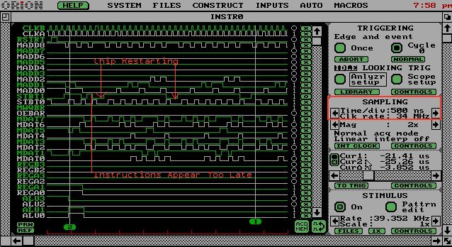
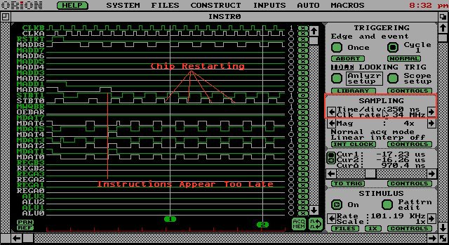
We increased the OMNILAB clock speed to 34 MHz (effective chip speed 8.5 MHz). Our results were
completely wrong. While the memory did provide the correct data for instructions, it appeared too
late for our chip to realize the instruction. This caused the chip to function improperly.
Finally, something apparently is causing the chip to restart every 4 or 5 cycles.
Below, we see multiply at 8.5 MHz.
Finally, we see memtest at 8.5 MHz. Again, the instructions appear too late, and the chip
gets in an endless loop of restarting itself.
Thus our prediction of 4.55 MHz maximum speed seems to be a good one. We observed complete
functionality at 4.25 MHz, but we ran into many problems at 8.5 MHz. We never tested with a
two-phase clock for the following reason: we tested at 8.5 MHz with a four-phase clock. We could
have run OMNILAB at 17 MHz with a two-phase clock, giving us an effective CPU speed of 8.5 MHz.
But our design relied on a delay between clock A and clock B; if it would not run at 8.5 MHz with
"clean" delays between clocks, we would not expect it to run at 8.5 MHz with no expected delay
between clocks. Two-phase clocking would offer us no insight into our chip's speed response.
Summary of Chip Results:
Chip #
5-15-30
Vdd10-25-35
GND10-30
GND-VddVerdict
1
2.4 ohms
1.8 ohms
17.4 Mohms
PASS
2
2.5 ohms
1.8 ohms
19.5 Mohms
PASS
3
2.1 ohms
1.7 ohms
2.1 ohms
FAIL
4
2.4 ohms
1.8 ohms
16.6 Mohms
PASS
5
2.3 ohms
1.9 ohms
18.0 Mohms
PASS
Test Name
Chip 1
Chip 2
Chip 4
Chip 5
add1path
PASS
PASS
PASS
PASS
insfunc
FAIL (*)
PASS
PASS
PASS
multiply
N/T
PASS
PASS
PASS
memtest
N/T
PASS
PASS
PASS
regpaths
N/T
PASS
PASS
PASS
countzeros
N/T
PASS
PASS
PASS
negate
N/T
PASS
PASS
PASS
infmux
N/T
PASS
PASS
PASS
mem2regpath
N/T
N/T
N/T
PASS
Failure Analysis:
No failures were observed for chips 2, 4 or 5. All three exhibited complete functionality on all
tests.
Chip 3 appears to have a short somewhere between Vdd and GND. This is most likely the result of a
fabrication flaw, since three of our other chips functioned perfectly.
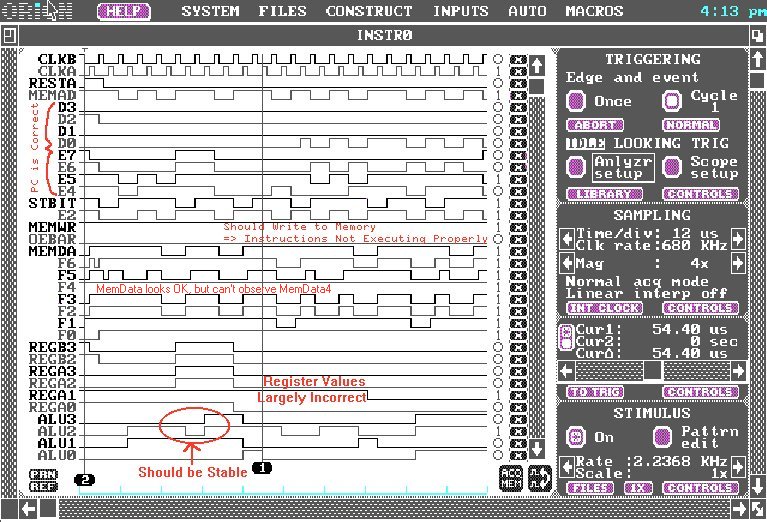
Before we connected our SRAM, we tested our CPU using our IRSIM vectors from last semester (i.e.
letting the stimulus go to HiZ when not writing to the chip). Chip #1 passed the
add1path test with complete functionality. We then tested Chip #1
using our insfunc test. It failed very badly. After the second clock
cycle of operation, essentially every internal value we observed was wrong.
Speed Testing:
All of the above tests were conducted at a clock rate of 680 kHz. Since we used a 4-phase clock,
our effective speed of operation was 680/4 = 170 kHz.