Hardware Setup
-
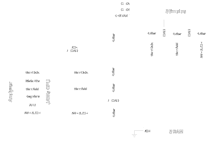
Our basic setup consisted of the stimulus, SRAM, analyzer, CPU, 7 SN74S241 Octal Buffers,
and 1 NAND chip. The stimulus provided loading of instructions into the SRAM as well as
clocks and RESTART for the CPU. The tri-stateable buffers separated the CPU memory
signals from the stimulus memory signals when the instructions
were being loaded into the SRAM. The enables for the buffers, ILOAD and /ILOAD, are
switched after the instructions are loaded into memory, so that the CPU can begin
operating. The use of the analyzer is clearly shown in the diagram below. The NAND chip is necessary to prevent fighting between the loop of buffers
that separate the bidirectional memory data lines of the CPU from the memory data
lines of the stimulus. Since both buffers in the loop could be driving values
before the instruction loading is finished, one cannot turn one of the buffers on
while the other is on. So after instruction loading is done, we can never turn
both buffers on to effectively create a wire between the SRAM and CPU because
there is never any assurance that the enables on the buffers can switch at exactly
the same time. Thus, our NAND gates are wired as to provide the control for using
the lines for two-way communication.
We used six sets of test vectors which tried to exploit possible stuck-at
faults as well as functionality flaws. We basically sent every possible logic
value across every possible data path to ensure that our chips were internally
working well (Note that A's and 5's are used heavily to test this in as few
instructions as possible). These types of tests display the correctness of our
chip to
a high degree because we have a great deal of observability at the pins (registers,
ALU outputs, memory data, memory address, and state bits).
These six sets of test vectors each had about ten or more instructions each.
They covered all instructions.
Since some aspects of our design, like the ALU and PC, we could not reasonably
test exhaustively,
we used
three programs which ran from 30-40 instructions each to gain a better confidence level
in our chip and its robustness.
Test Vector Overview
Functional Block Correctness