This test is designed to verify that the registers can all be accessed and written to. The file verifies that the read and writeback paths function properly for all logic values; it also shows that ImpReg3 passes all logic values correctly. Finally, this test verifies the latches in the register read and writeback paths.
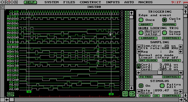
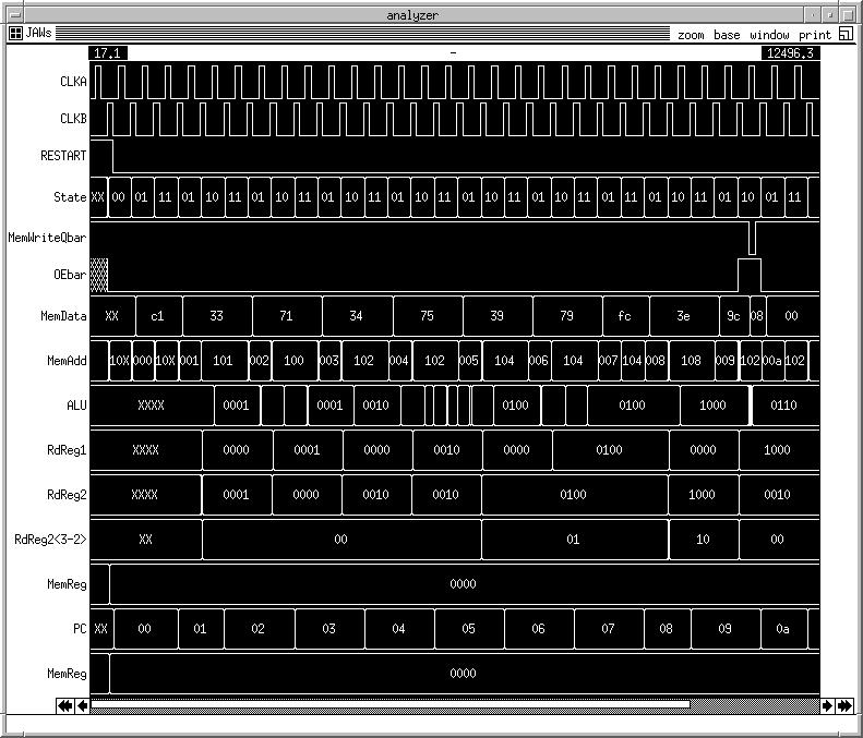
To verify functionality, we first looked at the result of the SW, making sure the chip provides the correct data and address to the SRAM. This verified most of the functionality; we also watched the PC and ensured that the registers always had the correct values for each instruction.
Chips 2, 4, and 5 all passed this test with complete functionality.
Instruction Sequence:
Restart of the chip ...
LDI  0001
OR   0011
SLL  0001
OR   0100
SLL  0101
OR   1001
SLL  1001
ZERO 1100
OR   1110
SW   1100
NOOP
| SRAM Test

logfile cpu.log

clock Vdd      1 1 1 1
clock CLKA     0 1 0 0
clock CLKB     0 0 0 1

| pin vectors
vector MemData MemData7 MemData6 MemData5 MemData4 MemData3 MemData2 MemData1 MemData0
vector iMemData iMemData7 iMemData6 iMemData5 iMemData4 iMemData3 iMemData2 iMemData1 iMemData0
vector MemAdd  MemAdd8 MemAdd7 MemAdd6 MemAdd5 MemAdd4 MemAdd3 MemAdd2 MemAdd1 MemAdd0
vector iMemAdd  iMemAdd8 iMemAdd7 iMemAdd6 iMemAdd5 iMemAdd4 iMemAdd3 iMemAdd2 iMemAdd1 iMemAdd0
vector State   StBit0 StBit1
vector RdReg1 RegA3 RegA2 RegA1 RegA0
vector RdReg232 RegB3 RegB2
vector ALU ALU3 ALU2 ALU1 ALU0

| pin ana's

ana CLKA CLKB Restart MemAdd  State MemWriteQbar OEbar MemData RdReg232
ana RdReg1 ALU Vdd
ana Trigger

ana ILOAD WE_L iMemData
|ana iMemAdd  <- not enough room on analyzer pins


V RESTART   0
V iMemAdd  000000000 000000000  000000000 000000001 000000001 000000001 000000010 000000010 000000010 000000011 000000011 000000011
V ILOAD     0
V ILOAD_bar 1
V WE_L      1 0 1  1 0 1  1 0 1  1 0 1
V iMemData 11000001 11000001 11000001 00110011 00110011 00110011 01110001 01110001 01110001 00110100 00110100 00110100
R
V iMemAdd  000000100 000000100  000000100 000000101 000000101 000000101 000000110 000000110 000000110 000000111 000000111 000000111
V iMemData 01110101 01110101 01110101 00111001 00111001 00111001 01111001 01111001 01111001 11111100 11111100 11111100
R
V RESTART   0 0 0 0 0 0 0 0 0 0 0 0 1 0 0
V ILOAD     0 0 0 0 0 0 0 0 0 0 1 1 1 1 1
V ILOAD_bar 1 1 1 1 1 1 1 1 1 1 0 0 0 0 0
V WE_L      1 0 1 1 0 1 1 0 1 1 1 1 1 1 1
V iMemAdd  000001000 000001000  000001000 000001001 000001001 000001001 000001010 000001010 000001010 111111111 111111111 111111111 111111111 111111111 111111111
V iMemData 00111110 00111110 00111110 10011100 10011100 10011100 00000000 00000000 00000000 11111111 11111111 11111111  11111111  11111111  11111111
R

V ILOAD     1 1 1 1 1 1 1 1 1 1 1 1 1 1 1 1 1 1 1 1 1 1 1 1 1 1 1 1 1 1 1 1 1 1 1 1 1 1 1 1 1 1 1 1 1 1 1 1 1 1 1 1 1 1 1 1 1 1 1 1 1 1 1 1 1 1 1 1 1 1 1 1 1 1 1
V ILOAD_bar 0
V WE_L    1
V iMemAdd  111111111
V iMemData 11111111
V RESTART 0
R