Functional Description of JAWs CPU:
-
We have designed a 4-bit CPU that uses load/store architecture, 4 4-bit
general purpose registers, 512 bytes off-chip memory, and 16 8-bit fixed
length instructions.
Objectives: Our main design objective was to create a chip that could run reasonably complex programs. That is we wanted our chip to be as useful as a 4-bit CPU could be in a computational sense. To achieve our goal we settled on a small instruction size of 1 byte, so that we could literally write larger programs for a given amount of memory. We also decided to implement 4 general-purpose registers as opposed to an accumulator, so that we could cut down on memory related instructions. Also, during the design of our instruction set we made conscious decisions to specialize certain instructions so that we could better achieve our design goal. Usually in such specialization issues you lose out on compiler simplicity, and you create the need for more hardware. However, we have no need for a compiler, and space is not a problem for a 4-bit CPU.
Instruction Set: Our instruction set has a 4-bit opcode and, correspondingly, 16 instructions (see instruction set table). Three bits of the opcode are also used as the opcode for the 4-bit ALU. Since we are using 8-bit long instructions and we have a 4-bit data path, we decided to use an implied register file address(reg3) when we are doing operations that use an immediate value. Also, our ALU instructions write back their result to the first operand’s register file address because we have limited amount of instruction bits. All of our instructions have a latency of 2-3 clock cycles (see state diagram) since we decided against a pipelined architecture.
ALU: We created a 4-bit ALU that has the following operations: add, add immediate, subtract, shift left logical, not, and, and or. We used a barrel shifter for our shift left. We also implemented a Manchester 4-bit adder to increase speed of the slowest path in our ALU. This ended up being a good idea because our adder path was the most critical path on our chip (not considering off-chip memory).
Memory: Our chip addresses 512 bytes of off-chip memory. The lower 256 bytes are used for instruction memory, and the upper 256 bytes are used for data memory. Note that since we have a 4-bit data path, we didn’t use the upper nibble of the 256 data memory bytes. If we needed the extra data memory we could have come up with some sort of mux strategy to utilize both nibbles. Since our data path is 4-bits and we have 8-bit addressable data memory, we make use of a special memory address register that provides the upper nibble of the memory address whenever a data memory access is made. This memory address register can be set by two different instructions.
50-word MOSIS Description
-
We have created a 4-bit CPU which uses load/store architecture. It has
four 4-bit general purpose registers. Its instructions are 8-bit
fixed length with a 4-bit opcode. The CPU addresses 512 bytes of
off-chip memory that is split between instruction memory and data memory.
Official Project Name: JAWs
Notes:
$reg denotes the bit string inside of the specified
register.
The purpose of each of the pins listed below is considered clear unless it
is explicitly stated.
Instruction Set
Mnemonic
Format
Functionality
ADD
0101AABB
regAA < = $regAA + $regBB
ADDI
0100AAAA
reg3 < = $reg3 + AAAA
SUB
0001AABB
regAA < = $regAA - $regBB
SLL
0111AABB
regAA <= $regAA << BB
NOT
0110AABB
regAA < = !$regBB
AND
0010AABB
regAA < = $regAA & $regBB
OR
0011AABB
regAA < = $regAA | $regBB
LW
1101AABB
regAA < = Memory Data at address [$MemAccessReg, $regBB]
LDI
1100AAAA
reg3 < = AAAA
SW
1001AABB
Memory Data at address [$MemAccessReg, $regBB] < = $regAA
SETMI
1000AAAA
MemAccessReg < = AAAA
SETM
1110AAXX
MemAccessReg < = $regAA
BEZ
1010AABB
if ($regAA == 0) then PC < = [$MemAccessReg, $regBB]
BGZ
1011AABB
if ($regAA > 0) then PC < =
[$MemAccessReg, $regBB]
NOP
0000XXXX
ZERO
1111AAXX
regAA < = 0000
Pin Assignment
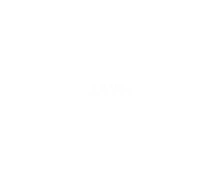
Outputs:
  ALU<0>
  ALU<1>
  ALU<2>
  ALU<3>
  RegB<3>
  RegB<2>
  RegA<0>
  RegA<1>
  RegA<2>
  RegA<3>
  MemAdd<7>
  MemAdd<6>
  MemAdd<5>
  MemAdd<4>
  MemAdd<3>
  MemAdd<2>
  MemAdd<1>
  MemAdd<0>
  OEbar:
    output enable for off-chip
    memory device
  MemWriteQbar:
    write enable signal for
    off-chip memory device
  StBit0
  StBit1
Inputs:
  GND
  Vdd
  RESTART
  CLKA
  CLKB


Input/Output pins controlled by
internal MemWriteQ signal:
  MemData<7>
  MemData<6>
  MemData<5>
  MemData<4>
  MemData<3>
  MemData<2>
  MemData<1>
  MemData<0>