Circuit Design and Logic Diagrams
The following is a description of the design of the basic elements of our design. We have included logic diagrams where the design was not necessarily obvious. The cell layouts and verification can be found in our cell hierarchy.
-
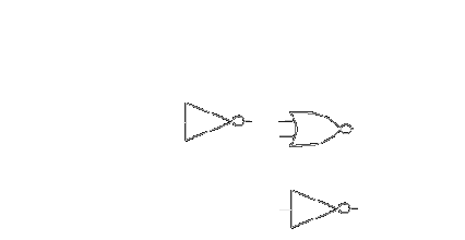
Latches - . We have two types of latches
which are used in our circuit. Both are resettable, and one has buffered
output. We used the one with buffered output in situations where there could
be possible corruption of data because of tgates. We alternate mirrored our
one bit latches to create 4 and 8 bit latches.
Below is a diagram of our buffered resettable latch.
Multiplexers - Our muxes are standard transmission gates type muxes instead of combinational, so we paid very close attention to their bidirectionality during the interconnection of our circuit elements.
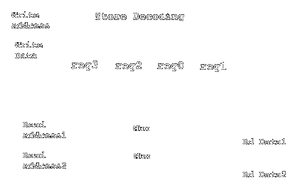
Registers -
-
Our register file consists of four groups of four bit latches which represent
four general purpose registers. The store input of each of the register 4-bit
latches is decoded from the write address input to the register file. The
outputs of the 4 registers are connected to two muxes which each take all four
registers as inputs. Reading from the register corresponds to selecting one
of the mux inputs through the read address inputs to the register file.
Add-one unit -
-
To increment our PC, we need to add 1 to an 8-bit number. We built a customized adder
for this.
The adder is comprised of 8 add blocks, each with 2 inputs: carry in and the input bit, and with 2 outputs: the sum bit and a carry out bit. The first block has a carry in of 1; subsequent blocks depend on the carry out of the previous block.
The following logic operations will be performed in each add block:
OUT = (IN XOR CIN)
COUT = (IN * CIN) = (IN' + CIN')'
We use the compound logic XOR, as described in class, for OUT; we use a NOR on the inverted inputs for COUT.
Zero Logic -
-
For our branch detection, we need to know whether the 4-bit two's complement number supplied
by the register file is equal to zero, and also whether it is greater than zero. Assume the number
is DCBA, with D as the MSB.
For the equals zero logic, we simply need to NOR all of the bits, as all bits must be zero:
EQZ = (D+C+B+A)'
which requires a 4-input NOR gate.
For the greater than zero logic, we must analyze the sign bit and OR the rest of the bits:
GTZ = D' * (C+B+A)
This simplifies to:
GTZ = ( D + (C+B+A)' )'
which uses a 2-input NOR gate and a 3-input NOR gate.
ALU -
-
Our ALU performs 2's-complement arithmetic on two 4-bit operands. The ALU
inverts both operands at the beginning, using either the inverted or the
non-inverted operand as appropriate per calculation. All "ALU operations" are
performed at once, in parallel, using the operands as described above. At
the output of the ALU, a multiplexer takes all of the ALU results and uses
the opcode to select the appropriate signal to output.
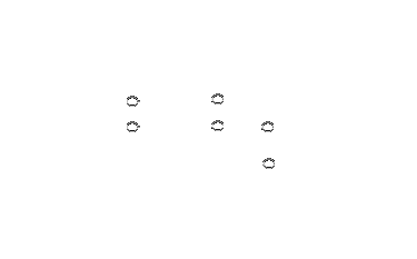
ADD - 4-bit Manchester adder
-
Our adder takes advantage of carry-lookahead techniques to increase
speed. The basic idea behind carry-lookahead adders is that you define a
generate and a propagate signal for the ith bit adder cell. The generate
and propagate signals are only dependent on the ith bit values for the
operands A and B. The generate signal produces a one when a carry out is
definetely going to be asserted. The propagate signal produces a one when
the ith bit values for A and B are such that they would "propagate" a carry
when the bit adder cell received a carry in.
Gi = Ai & Bi
Pi = Ai + Bi or Ai (+) Bi (since the generate covers Ai & Bi)
This leads to
Ci+1 = Gi + (Pi & Ci).
This definition of the generate and propagate signal leads to the fact that the generation of all carry bits can be accomplished in two levels of logic. This follows from the sum of products which arises from the recursive relation of the carry bits given above.
The sum for each bit adder cell can then be written as
Si = Ci-1 (+) Ai (+) Bi.
The Manchester Adder physically distributes the carry signals perpendicular to the data flow from the operands to the sum. We created a one bit adder, and then alternate mirrored them in a stack.
Below is a logic diagram of a single bit cell for the adder.
SUB - invert the bits of the second operand, set the carry in for the adder to 1. (The carry-in bit will be one bit of the op-code). A mux on the B input for the Manchester Adder determines whether B or B' is fed in. The mux control is also a hardwire from the ALU op-code.
NOT - use 4 inverters (one per bit)
AND - use a NOR on the inverted operands
OR - use a NAND on the inverted operands
SLL - use a 2-4 decoder with our previously designed barrel shifter. Literal<2-0> will be zeros. High bits will the the value from the register. We also reverse the order of our shift controls.
Since our instructions take varying amounts of clocks to complete, we have performed our timing
analysis on a per instruction basis. Our timing discipline then allows us to have valid timing
for instruction after instruction as long as we make sure that each instruction's timing will not
effect a following instruction's timing.
The timing of the instructions can be broken up into groups of instructions which have common
timing and data paths. The groupings of signals primarily serve for clarity
in the diagrams. Certain signals controlling a particular datapath may not be
labelled; however, the context of the instruction or grouping should make the
situation clear. Also, some latches are labelled with signals which are stable
over several clock periods. The state diagram is very helpful to look at when
trying to make sense of the stable periods.
Since a CPU cannot be easily tested for all possible operations, brute force
methods are exchanged with more thoughtful ways of establishing whether the
chip works as hoped. Our methodology here was to establish that all of our
data paths transmitted data to their destinations (latches, outputs, ...)
correctly. That is to test that all paths properly transmit all
possible logic values. Note that interconnection problems resulting from
a transmission gate's bidirectionality are discovered when performing this
testing because we pay careful attention to the destination of the
data flow. After establishing the correctness of the data flow and
of the interfacing of subcells, we can rely on the fact that our sub cells have been verified. We then ran some small programs and sequences of instructions
to further test the functionality of our chip.
Note that our testing here is performed on an unflattened version of our
layout, so we have included signals which do not appear at the pins. This
is done for the purpose of clarity.
After we finished testing the non-flattened CPU, we changed the command
files from below so that only pin signals were logged to the log file
using 'w'. We then generated log files from both our flattened and
non-flattened layout using the new command files. We checked to make sure
that the simulations were
identical using the file comparison program diff. Thus, we were ensured
that our final simulations look exactly like the simulations below when
one restricts attention to pin signals.
We also ran test vectors which interrogated specific functionalities of
our chip. These tests including running the instructions which we didn't
use in our testing above.
We also tested a couple of small programs which perform useful operations.
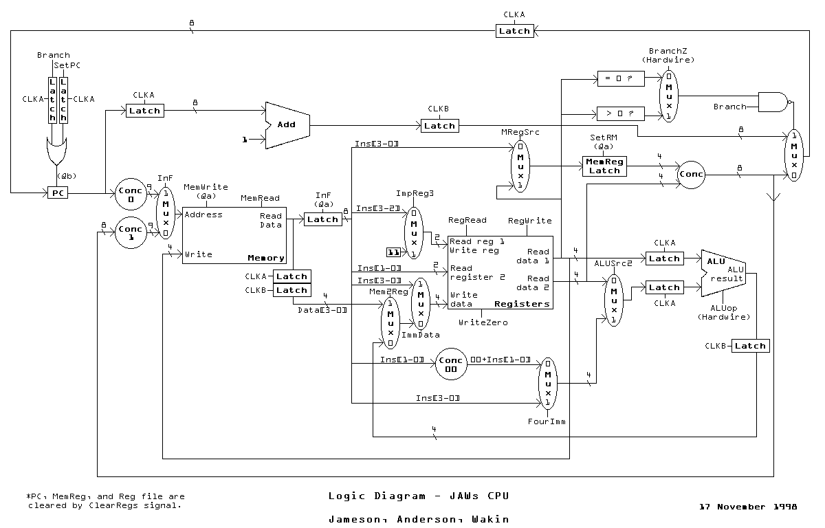
Logic Diagram
System Timing
Timing Group
Instructions in Group
ALU
ADD, ADDI, SUB, AND, NOT, OR, SLL
Branch
BGZ, BEZ
Load
LW
Load Immediate
LDI
Store
SW
Set MemReg
SETM, SETMI
Zero Register
ZERO
No Operation
NOP
IRSIM Results - Subcells
Our cell hierarchy contains IRSIM results for all subcells of the
JAWs CPU.
IRSIM Results - JAWs CPU
Testing Methodology
Implementation
To establish the correctness of the data flow, we propigated A's and 5's
through all buses to make sure that each bus line was able to transmit both
a one and a zero. In some cases it was more beneficial to using walking 1's
on a bus. This basically meant that we were seeing if latches
latched properly, if mux lines functioned properly, and if the wires
themselves were routed properly.
Paths Verified (click for irsim results and command files)
Functionality Tests