Crystal | Longest Path | Spice | Clock Frequency
We performed Crystal analysis on the following cells. We extracted as much useful information as was possible from the crystal results regarding logic levels for inputs we did not specify. When possible, these are noted below. The times listed indicate the critical path for each cell.
We deduce from these results that the longest path will be through our ALU.
Specifically, we expect the following results from the 4-bit Manchester Adder:
READING:
Because the register values are legitimate when a read cycle begins, we need
only wait for the mux control signals to choose among the registers for the
regfile output. This is approximately the delay of one regfilemux, or 3.90ns.
Register reads will be performed much more quickly than ALU operations.
As circuit elements contributing to the longest path, we have analyzed the
following cells (in their respective top-levels) with Spice. The inputs were
chosen to correspond to the ALU worst-case documented above.
(*) We were unable to produce useful Spice results for the ALU output mux,
possibly because of its t-gate design.
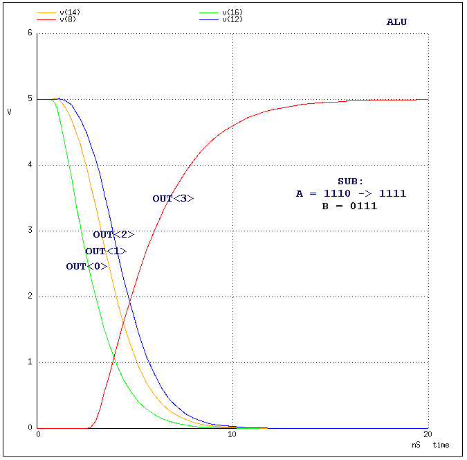
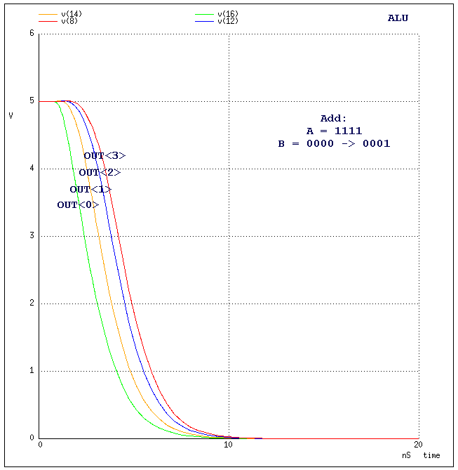
We were, however, able to run Spice on the entire ALU, for the worst-case
scenario as described above. The results agree
quite closely with the Crystal prediction of a 10ns delay.
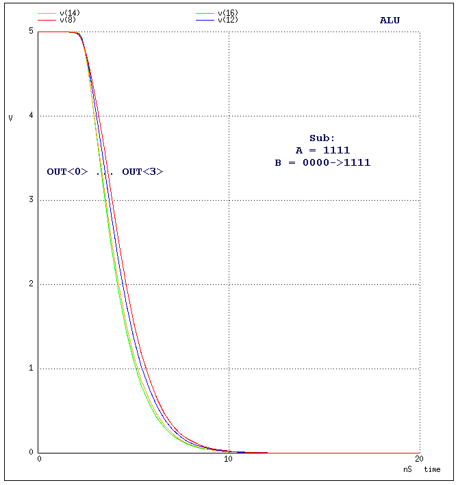
Outside of our worst-case scenario, we performed the following Spice analysis:
In designing our CPU, we anticipated the longest path coming from the ALU.
We also operated under the assumption that our 2-phase clocks would have
25% duty cycles and would be evenly spaced. Noting that our ALU was part of
a feedback path needing A and B latches, we placed one latch immediately before
the ALU, and one immediately after it. This allowed for the ALU to absorb a
lot of the extra time between latching on A and latching on B. To minimize this
"ALU-type delay", we did not include any other combinational logic between
those two latches.
So, the ALU inputs are available on the falling edge of clock A, and the
outputs must be determined by the falling edge of clock B. Thus, one-half
our clock period must be at least 10.07ns. Our clock period must then be
at least 20.14ns, giving us a maximum theoretical clock speed of
In reality, though, the pad frame may not support such high clock speeds.
Another factor which we have neglected to mention is the delay invloved in
an off-chip memory write/read. Despite our initial assumption that the read access time would be our critical delay, it turns out that the minimum write pulse width
for our memory device will be the limiting factor in our clock speed. Because
our write enable signal is qualified with A, our minimum clock period must be
four times the minimum write pulse width.
With the SRAM specs we were given, the best-case write pulse width given was
55ns. This would bring our maximum theoretical clock speed down to
Crystal Analysis
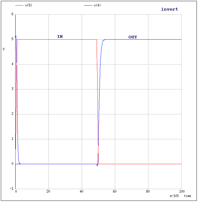
Inverter (invert)
: delay in -1 0
Node out is driven high at 0.22ns
: delay in 0 -1
Node out is driven low at 0.22ns
2-input NAND (2nand)
: delay A 0 -1
Node OUT is driven low at 0.50ns
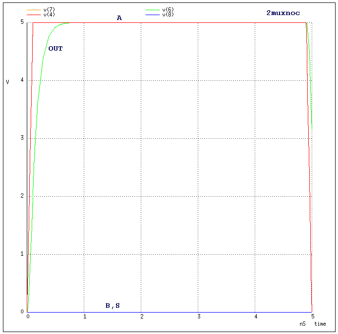
2-input, 1-bit mux (2mux)
A=1, S=0, SBAR=1
: delay A 0 -1
Node OUT is driven high at 1.26ns
For A or B
2-input, 9-bit mux (2mux9bus)
A<0>=1, S=0, SBAR=1
: delay B\<0\> 0 -1
Node Y<> is driven high at 1.30ns
Any A or B
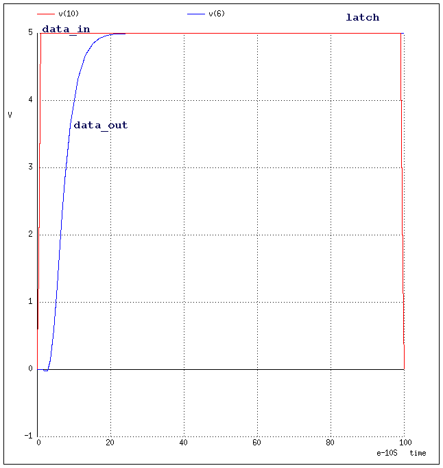
1-bit Latch (latch)
data_in=1, store=1, storebar=0, reset=0
: delay data_in 0 -1
Node data_out is driven high at 5.16ns
4-bit Transmission Gate (4b_tgate)
IN=0, data to pass=0
IN rise or fall
Node tgate_3/pass is driven high at 0.53ns
2-to-4 Decoder (2to4_decoder)
IN1=0, IN0=1
: delay IN1 -1 0
Node OUT0 is driven high at 1.69ns
4-bit Shift Register (4b_shift_contacts)
literal<6>=1, S<3>=1, SBAR<3>=0
: delay literal\<6\> 0 -1
Node OUT<3> is driven high at 3.13ns
(when any literal goes high)
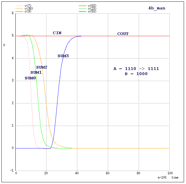
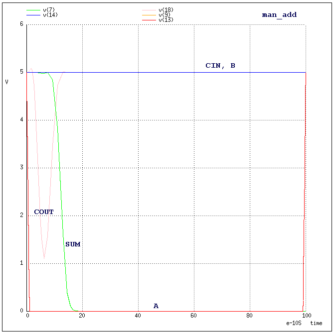
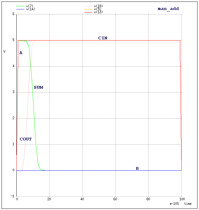
Manchester Adder - 1-bit Cell (man_add)
A=1, B=0, CIN=1
: delay A -1 0
Node COUT is driven high at 3.35ns
: delay B -1 0
Node COUT is driven high at 3.35ns
(when A or B goes low)
Register File - 4-input, 4-bit mux (regfilemux)
: delay A0 0 -1
Node OUT<0,2> is driven high at 3.90ns
Longest Path
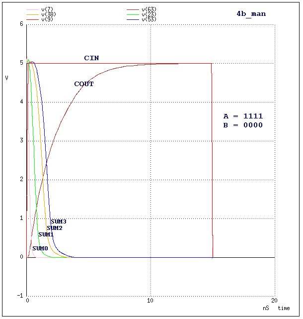
   B0=0, B1=?, B2=?, B3=1, A0=1, A1=1, A2=1, A3=1, CIN=1
   For bit 0 COUT=1   3.35ns
       bit 1 COUT=1  <1.57ns
       bit 2 COUT=1  <1.57ns
       bit 3 COUT=1   1.57ns
   overall: SUM3 is driven high at 8.06ns
This is longer than any other ALU operation (shift, for example). So, noting
that we need a carry-in of one, and recalling that the bits of the B operand
must be inverted before being added to A when performing a SUB operation, we
conclude that the subtract operation will be our longest delay, more precisely
in the case where A transitions from 1110 to 1111 and B = 0111.
When performing this operation, we expect the following delays:
   invert            0.22ns   (Invert B operand)
   mux<0>           <1.26ns   (Select B' as input to adder)
   4b_man            8.06ns   (Add A+B'+CIN, where CIN=1)
   4b_decoded_tgate  0.53ns   (Select Adder result as ALU output)
   overall: OUT3 is driven high at 10.07ns
We mention briefly why the register file was not considered as a candidate for
our longest path:
WRITING: Even though there is a path which must be completed in a
quarter of a clock cycle because the latch's store signal is qualified, crystal
analysis of each of the gates contributing to that path leads us to believe
that it will not be a problem.
Spice Analysis
Clock Frequency
1 / (2*10.07ns) = 49.7MHz.
1 / (4*55ns) = 4.55MHz.