Overview | Cell Hierarchy | Full Plot | Floorplan
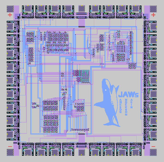
We settled upon some standards for our subcell design. All p-channel transistors had a 2x6 L/W ratio to achieve more symmetric rise/fall times. Most leaf cells had a standard height of 48 lambda.
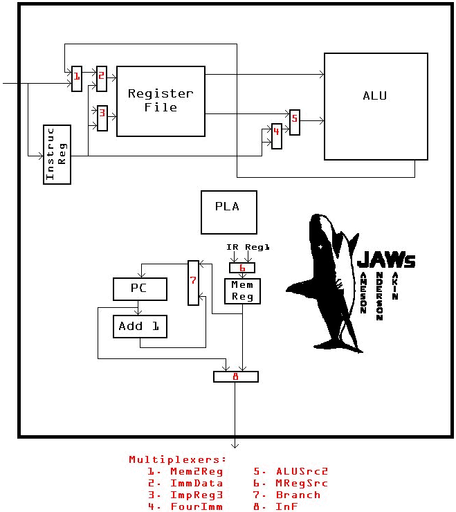
In our top-level CPU layout, as a general rule, we ran metal1 vertically and ran metal2 horizontally. This made layout much easier, since we knew what we needed to leave room for, and that by following the standard, we would not be trapped at some time in the future. While arranging the subcells in the top-level of our CPU, we tried to consider which signals needed to be routed to the I/O pads. We placed our PLA in the center of our chip, to make all control signal paths approximately the same length.
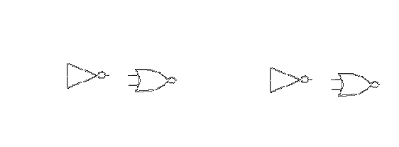
We discovered an unexpected problem with having 2 latches in series. We were noticing occasional data corruption of the signal between the latches, which is the data stored in the first latch. Our theory was that the first t-gate of the second latch started passing data before the second t-gate was cut-off. In general, this would only cause temporary fighting, but because the input of the second latch was connected directly to the feedback path of the first latch, there was a possibility that the stored value would be corrupted. The reason that the first t-gate would be turned on before the second would be turned off is that the inversion of the control signal would cause skew between store and storebar. The suspected problem is shown below:
Based on our theory, we were led to believe that buffering the output of the first latch would prevent such data corruption. This buffer solved the problem in all cases where we observed it. This leads us to believe that our theory for the cause of the data corruption was correct.
Click here to see the cell hierarchy,
including magic layout and
IRSIM test results for all subcells of
the JAWs CPU.
Cell Hierarchy