This page contains diagrams and explanations of the logic implemented
in our ALU chip. Components of primary concern are the following:
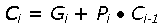
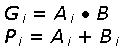
The carry look-ahead adder was chosen as an optimum balance between circuit real estate and speed. The current carry Ci is calculated by the following formula:
where:
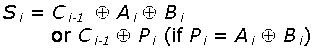
The sum Si is calculated by the following formula:
In the case that a negative number is added (i.e. 3 + (-6) = ?), the carry-in value is set to one. This is because in two's complement, negation is achieved by inverting bits and adding one (the carry-in). Otherwise, the carry-in value defaults to zero.
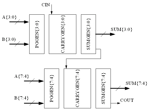
The following image provides a top-level look at the logic implemented in our adder.
We have also included the following logic and magic layouts of the adder subcomponents.
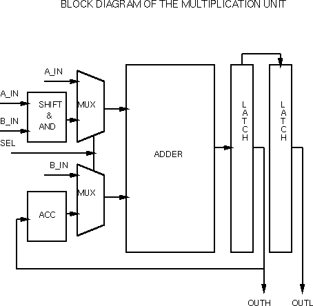
The algorithm used for multiplication is serial. The component takes two 8-bit numbers and performs multiplication in 8 clock cycles. Below is the block diagram detailing the process by which the multiply operation is performed.
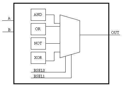
The above diagram shows the pattern for each bit of the Boolean unit; the unit as a whole is "embarassingly replicated". That is, each bit of the unit's output is dependent only on the corresponding bit of the inputs to the unit. The BSEL inputs (generated by the control block) determine which of the Boolean outputs to consider active in a given cycle.
We have also included the following magic layouts of the boolean subcomponents.
Last Updated: December 13, 1996